EE 420L Engineering Electronics II Lab - Lab 6
Nha Tran
03/15/2015
NSHE: 2000590233
trann4@unlv.nevada.edu
Single-Stage Transistor Amplifiers
- Below are schematics for NMOS and PMOS source followers amplifiers (also known as common-drain amplifiers).
- In your lab report discuss the operation of these circuits.
- Simulate the operation of these amplifiers.
- Hand
calculate, and then verify your hand calculations with experimentation
and simulations, the gains and the input and output
resistances ensuring that your test signals are at a high enough
frequency that the caps have negligible impedance but not so high that
the gain is dropping off.
- If
you build this circuit using electrolitic capacitors, assuming the
input AC signal swings around ground, put the "+" terminal of the cap
on the gate of the MOSFET. Please indicate, in your lab report, that
you understand why the capacitor is connected this way.
We
used electrolitic capacitor in our circuit and we connect the terminal
with the higher potential is positive and the lower potential is
negative.
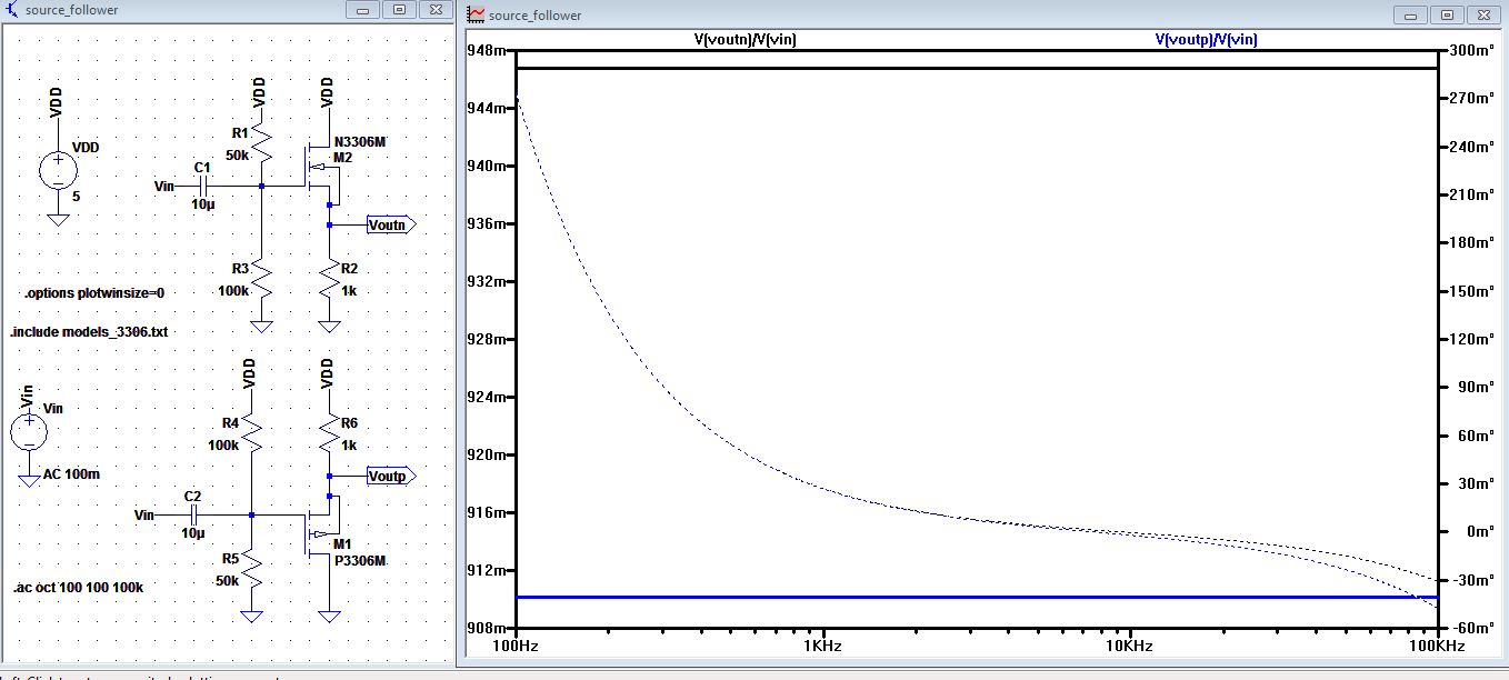
| Simulations for the gain of the source follower amplifier. |
| The transient analysis along with the circuit was drafted by Dr. Baker it shows that the gain for the Nmos = Pmos =1. |
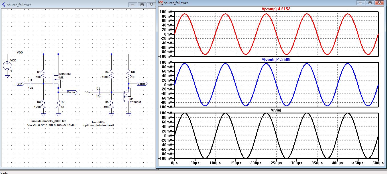 |
| Doing
the AC analysis and taking the reading at 10 kHz. The gain for
Voutn/Vin = 0.946. And the gain for Voutp/Vin = 0.910. Both roughly
equals 1. |
 |
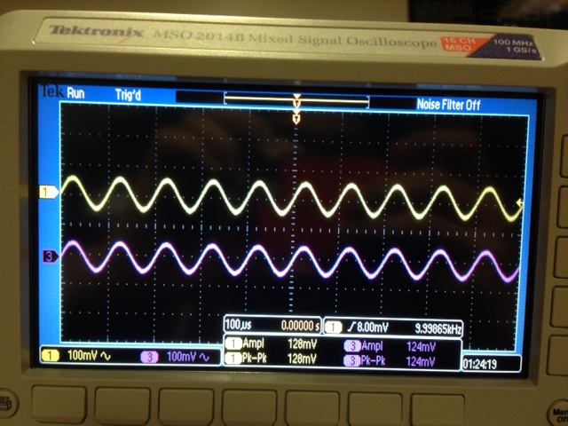
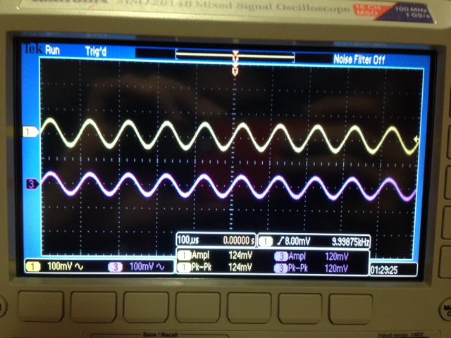
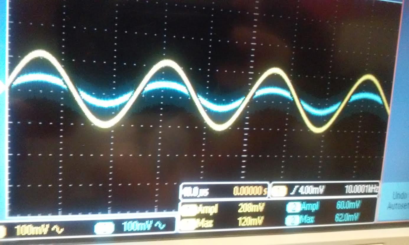
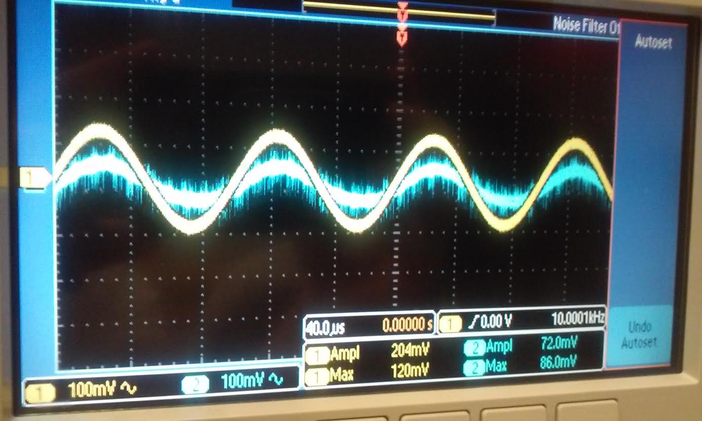
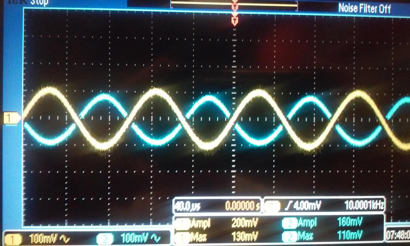
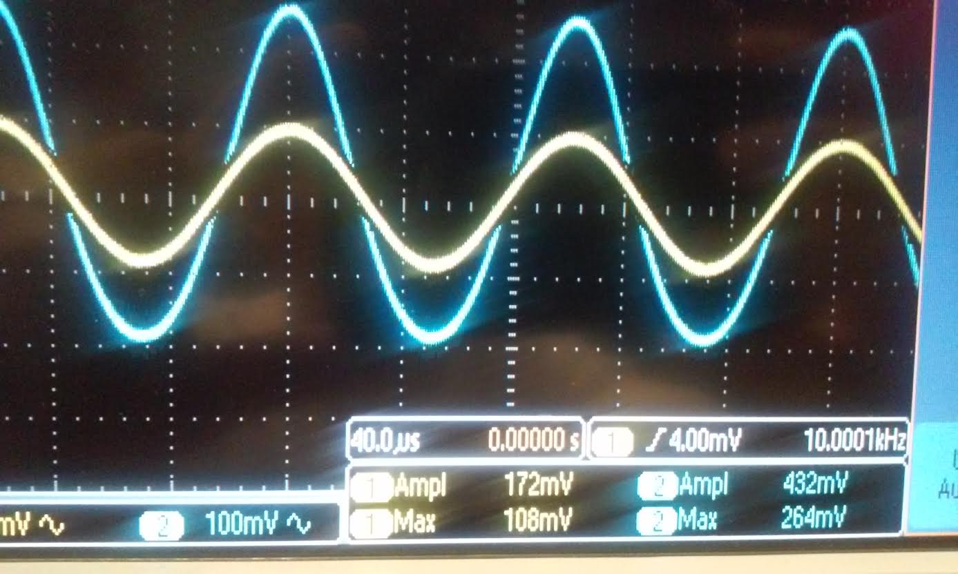
| Experimental scope reading of the gain for Voutp and Voutn |
| Voutn: as
you can see the the reading below the output matches the input so the
gain is 1, which is the same as our simulation and hand calculation | Voutp: vout is approximately Vin so vout/vin=1 |
 |  |
- In your lab report discuss, in your own words, how to measure the input resistance.
- For measuring the input resistance add a resistor equal to the value you calculated between the input voltage source and the amplifier.
- Measure
the peak AC current through this added resistor by taking the
difference in the peak AC voltages across the resistor (on one side is
the input voltage signal and the other side is the connection to the
amplifier's input capacitor) and then dividing by the resistor's value.
- Measure the peak AC voltage on the input of the amplifier (the left side of the capacitor).
- Dividing this peak AC voltage by the peak AC current through the added resistor is the amplifier's input resistance.
To
measure the input resistance we see that the resistance before Vin is
100k|| 50k, both are connected to AC ground so the input resistance is
33k. to measure the input resistance of the circuit we have to put 33k
resistance right after our input, but before the 100l|| 50k that way
the input amplitude gets divide in half before the signals goes into
the amplifier. the result of this is that our output should be half of
what it would have been if we did not added the 33k resistor. in our
case we should see the output is ~.5V, since we original output was ~1V.
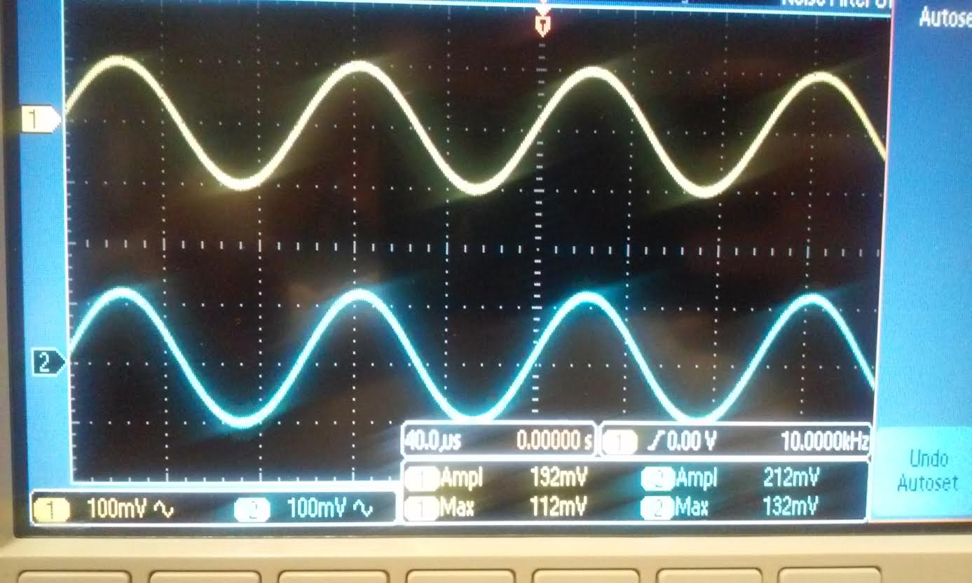
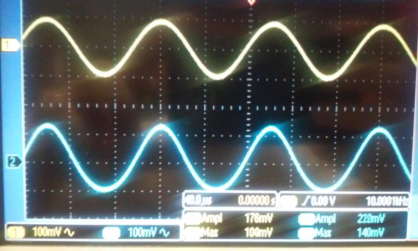
| Simulation and experiment of Rin |
| As
you can see below the Voutp/Vin and Voutn/Vin is now roughly half of
what it was before when a 33k resistor is placed before the capacitor. |
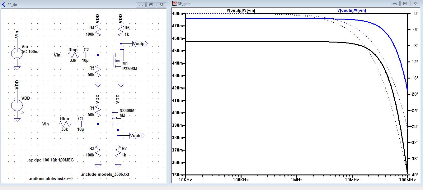 |
| Nmos: in the experiment we placed a 33k resistor at the same position as the schematic and we got Voutn/Vin is roughtly half | Pmos: same as the Nmos side |
 |  |
- Again, in your lab report discuss how to measure the output resistance.
- For
measuring the output resistance, add a resistor equal to the value you
calculated in series with a big capacitor (to avoid messing up the
biasing) from the amplifiers output to ground.
- Measure the peak AC current through this added resistor.
- Measure
the peak AC voltage (remove the DC component) on the gate of MOSFET and
the peak AC voltage on the source of the MOSFET. The difference in
these two AC voltages is the peak AC gate-source voltage of the MOSFET.
- Dividing
this peak AC gate-source voltage by the peak AC current through the
added resistor is the amplifier's output resistance.
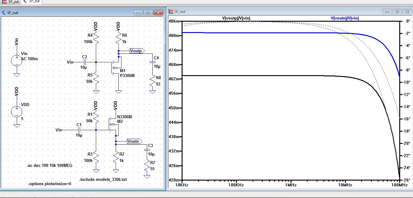
To
measure the output current we use the calculated values and add them in
series with a 10u capacitor, and we connected in parallel to the 1k
resistor for the Nmos and for Pmos we add it parallel to the Pmos
device. From the hand calculation we got 55 Ohms and 93 Ohms for the
Nmos and Pmos respectively. You can see from the schematic below how to
hook up the calculated Rout to get the desired results.
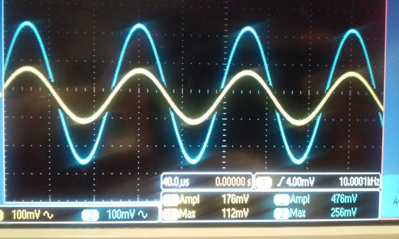
| Simulation and experiment of Rout |
| As
you can see when we hooked up 55 Ohms and 93 Ohms to the output of
Voutn and Voutp our gain Voutn/Vin and Voutp/Vin is roughly half of 1. |
 |
| Nmos | Pmos |
 |  |
| Summary: Nmos |
| Hand Calcution | Simulation | Experimental |
| Gain | 1 | 0.946 | 0.968 |
| Rin | 33k Ohms | 33k Ohms | 33k Ohms |
| Rout | 55 Ohms | 55 Ohms | 62 Ohms |
| Summary: Pmos |
| Hand Calculation | Simulation | Experimental |
| Gain | 1 | 0.910 | 0.969 |
| Rin | 33k | 33k | 33k |
| Rout | 93 Ohms | 93 Ohms | 390 Ohms |
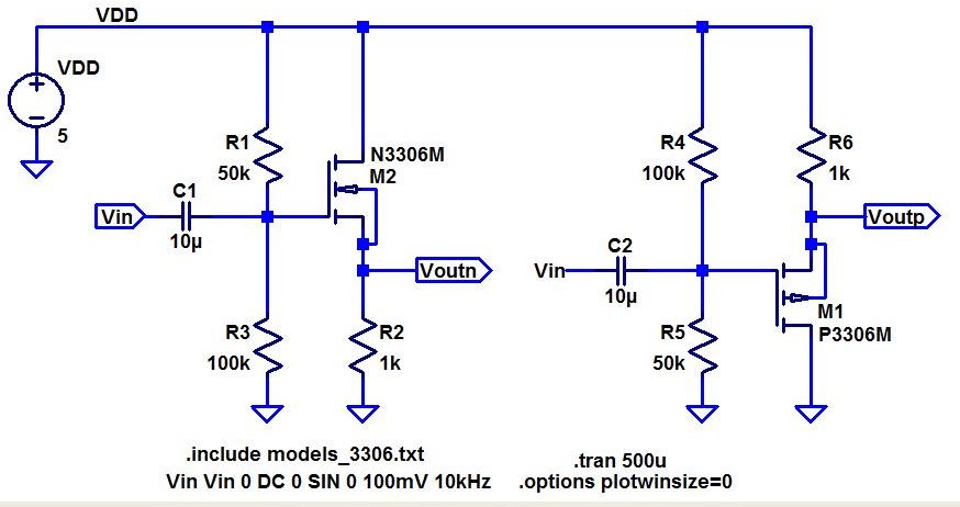
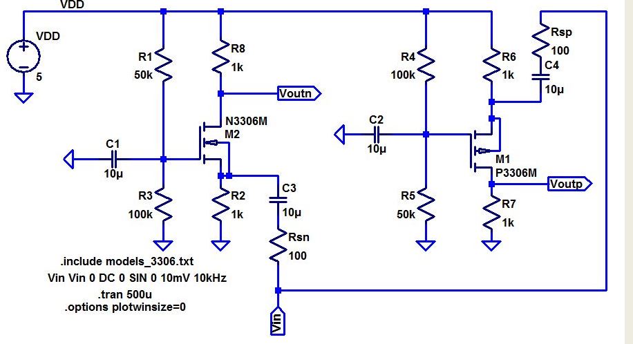
- Below are two common-source amplifiers.
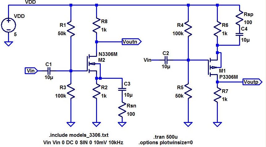
- Discuss the operation of these amplifiers in your lab report including both DC and AC operation.
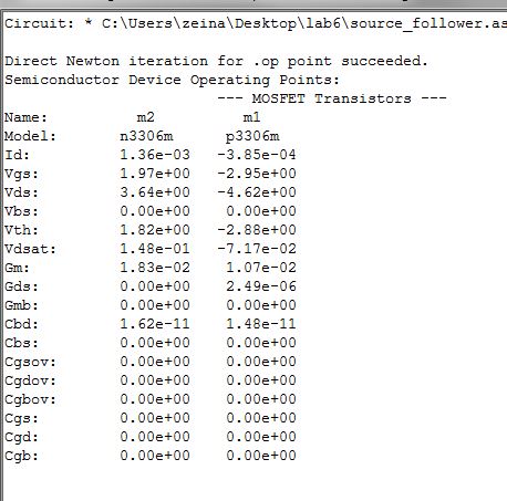
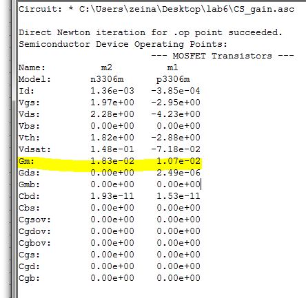
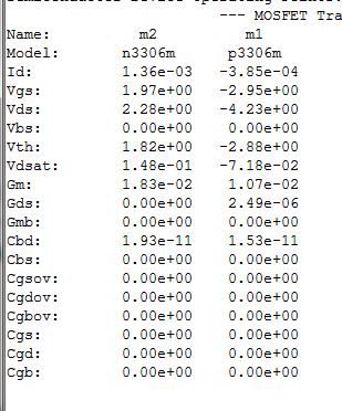
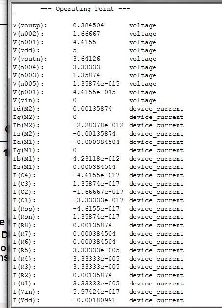
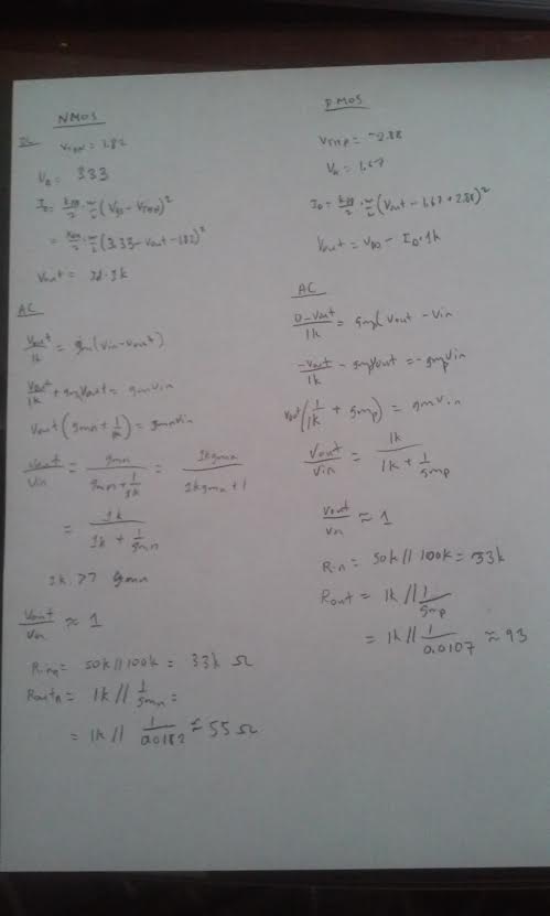
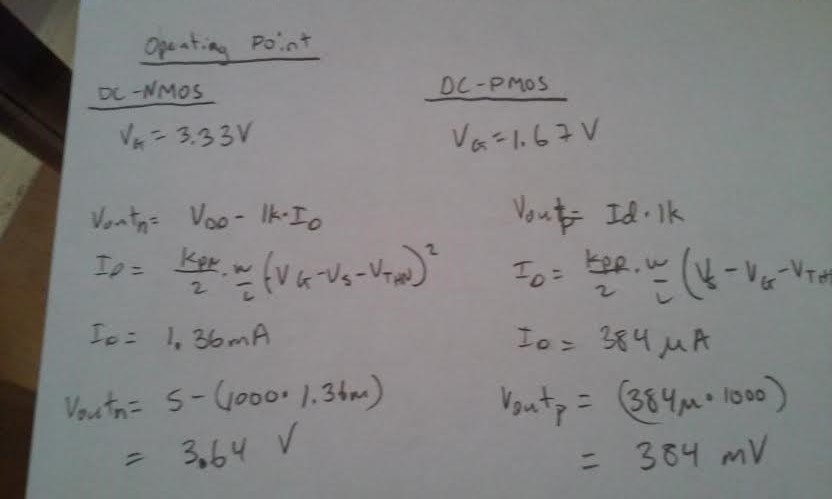
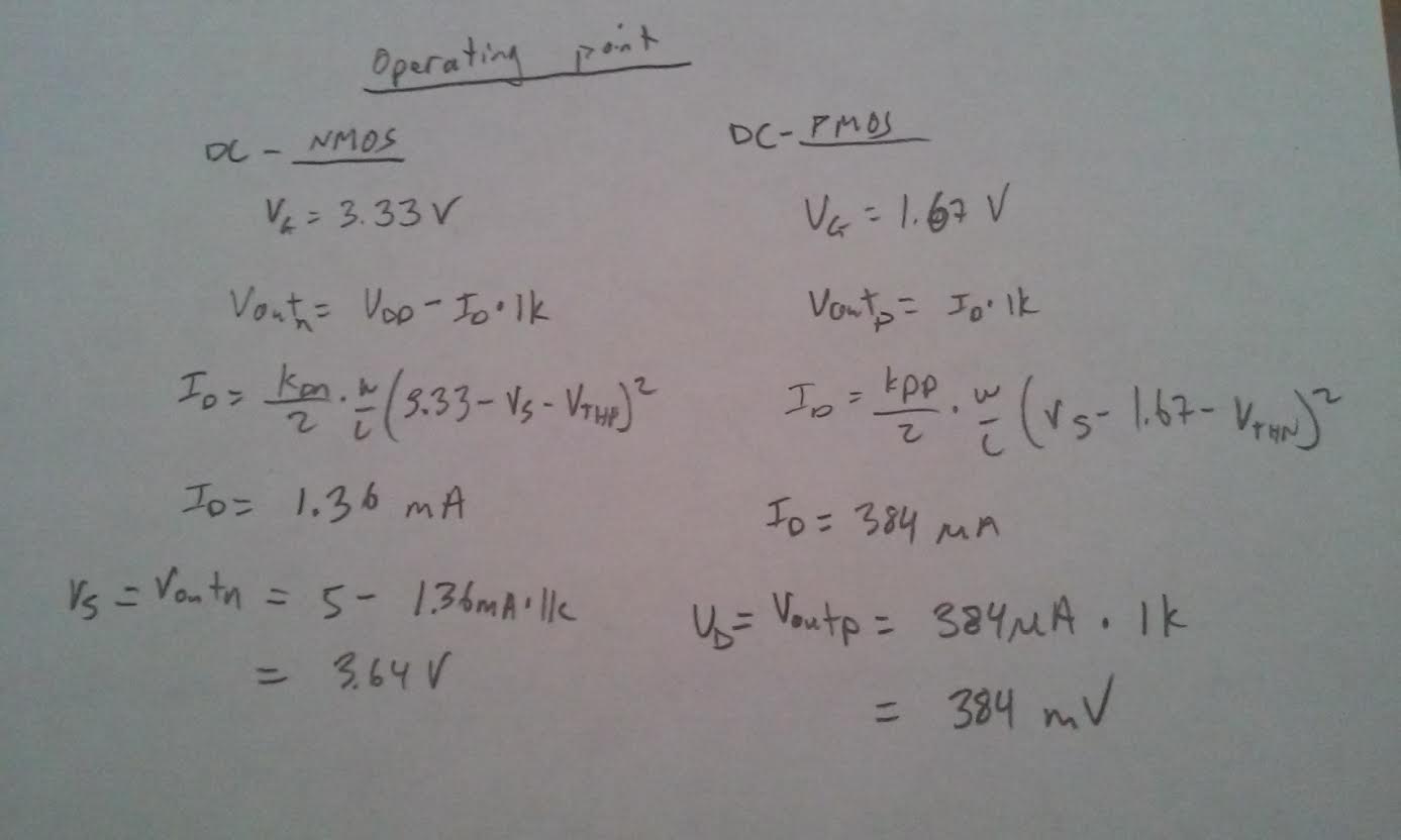
The DC operating point for the NMOS from looking at the
spice error log and the hand calculation below you can see that
gm=18.3mA/V, and Vout =VDD-id*1k = 3.64V. for the PMOS side the gm is
10.7mA/V and Vout =id*1k = 384mV, the threshold voltage is also taken
from the spice error log its value is 1.82V for Nmos and -2.88V for
Pmos. For AC vdd = 0V, so the operating point Rout and Rin is
limited by the 1k resistor and 50k||100k. Vin and Vout will be limited
by the hand calculations of the gain for AC below.
- Hand calculate the gains and the input/output resistances.
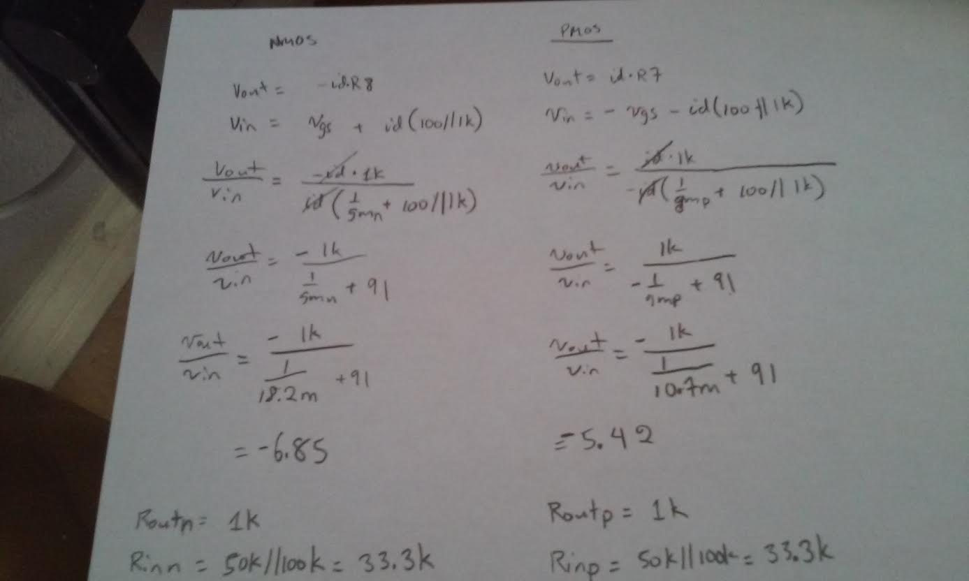
- How does the source resistance, Rsn or Rsp, influence the gain.
If we increase Rsn or Rsp then the gain will decrease.- Again compare your hand calculations to simulation and experimental results.
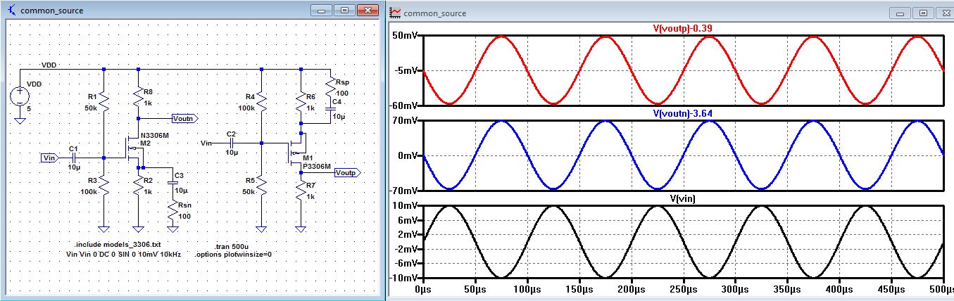
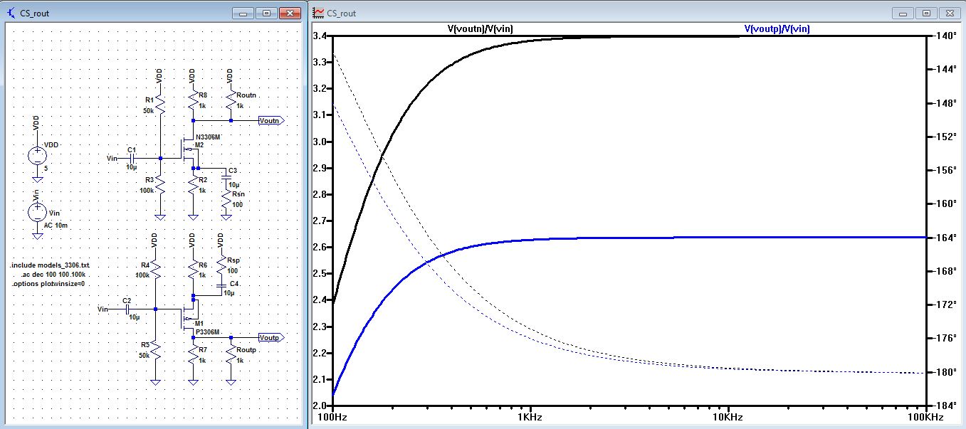
| Simulation of a common-source amplifier using LTSpice |
| From
the transient analysis below we can clearly see that the output of
Voutn = 50mV and Voutp = 70mV, and Vin. The Gain is Vout/Vin so the
gain is 5 for the Pmos and 7 for the Nmos amplifier. This circuit along
with the plot was drafted by Dr. Baker used in prelab. |
 |
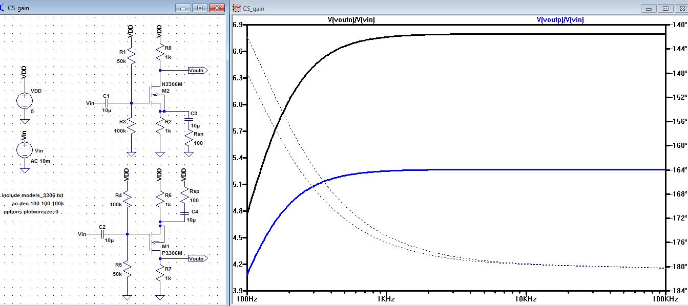
| We
can also verify the gain using an AC analysis. Below you can see that
the gain Voutp/Vin = 5.2 and Voutn/Vin = 6.7 at 10kHz. For the purpose
of the lab we can assume that the gain
is 5 and 7 respectively. The solid line is the magnitude of Vout/Vin,
and the dotted line indicate that phase, as you can see the phase for
both Nmos and Pmos is -180 degree. |
 |
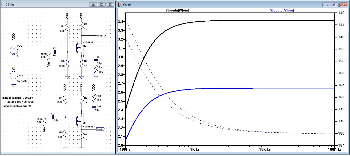
| From
our hand calculation, we got Rin was 33k Ohms for both the Nmos and
Pmos, so in theory if we put a 33k resistor in parallel before the 10u
capacitor we should get half of the gain we had from previous
simulation. You can see the schematic below a 33k resistor was placed
before the 10u capacitor and our new gain is roughtly half of what it
was before for both the Nmos and Pmos. This voltage division indicated
that our hand calculation of Rin=33k is correct. |
 |
| From
our hand calculation, we got Rout was 1k Ohms for both the Nmos and
Pmos, so if we put a 1k resistor in parallel with R8 for the Nmos, and
1k resistor parallel with R10 for the Pmos we should get half of the
gain. As you can see from the schematic below the location of Routn and
Routp, and the AC analysis gave us 3.4 for Nmos and 2.6 for Pmos, this
is half of our original gain. This voltage division indicated that our
hand calculation of Rout=1k is correct. |
 |
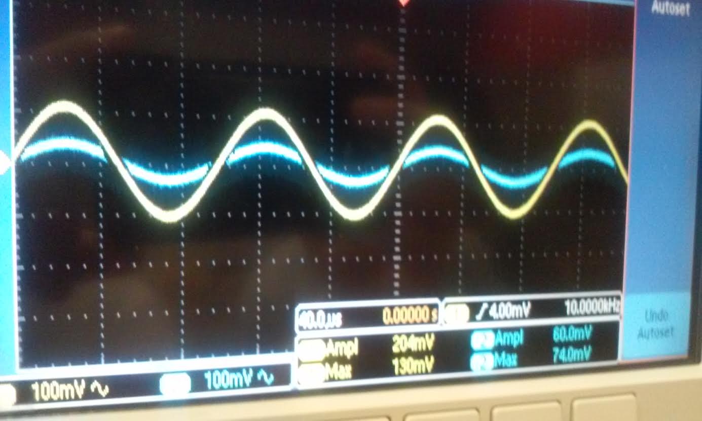
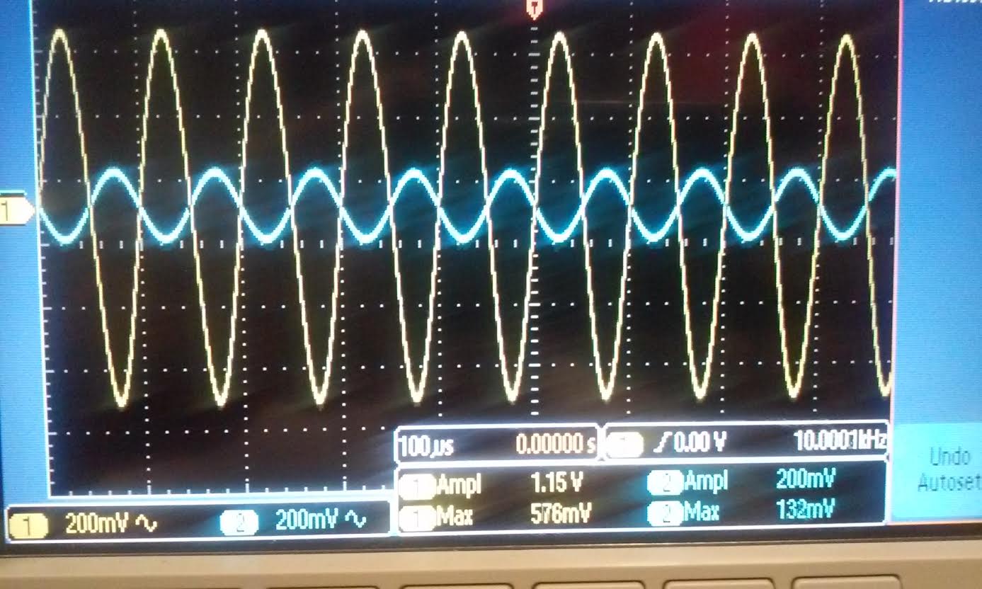
| Experiment of the NMOS and PMOS common-source amplifier |
| NMOS | PMOS |
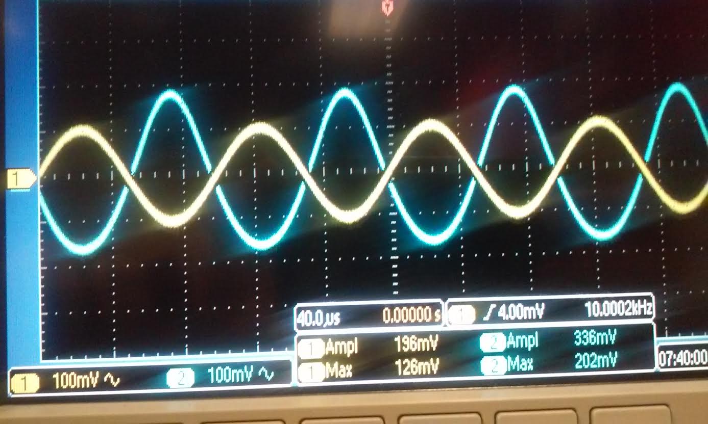
| Gain:
for the Nmos amplifier the gain is 1.15V/200mV = 5.75. For the Pmos the
gain is 336mV/196mV = 1.7. This gain is less than the theoretical
values which indicated that the Gm is much smaller than the expect
value of 10mA/V. In the data sheet of the ZVP3306A the forward
transconductance (gm) operating point is 60mS while our simulation was
only 10.7mA/V. it also gave the operating condition for Vds = -18V and
id=-200mA. Our Vds operating point was 4.6V and id was only 384uA. |
 |  |
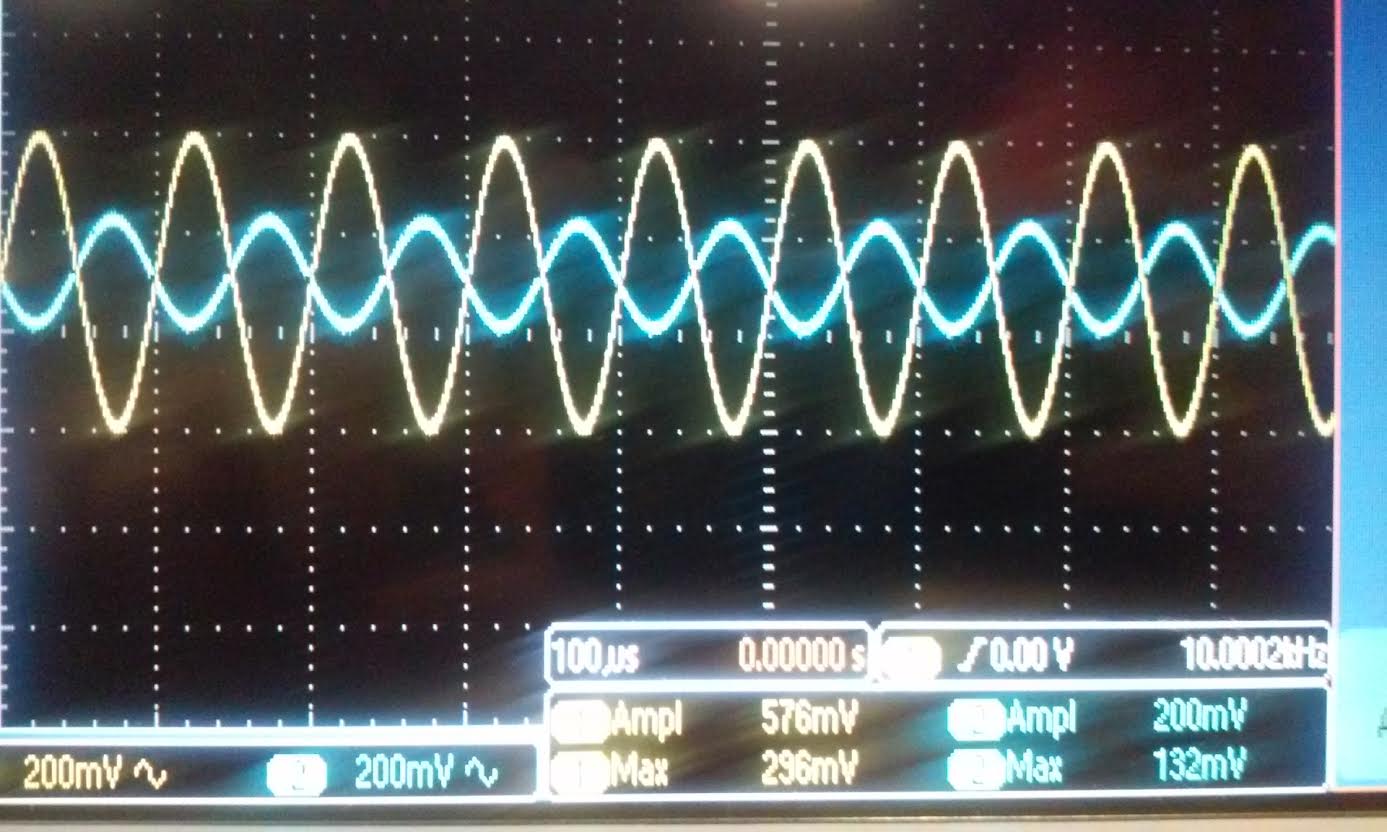
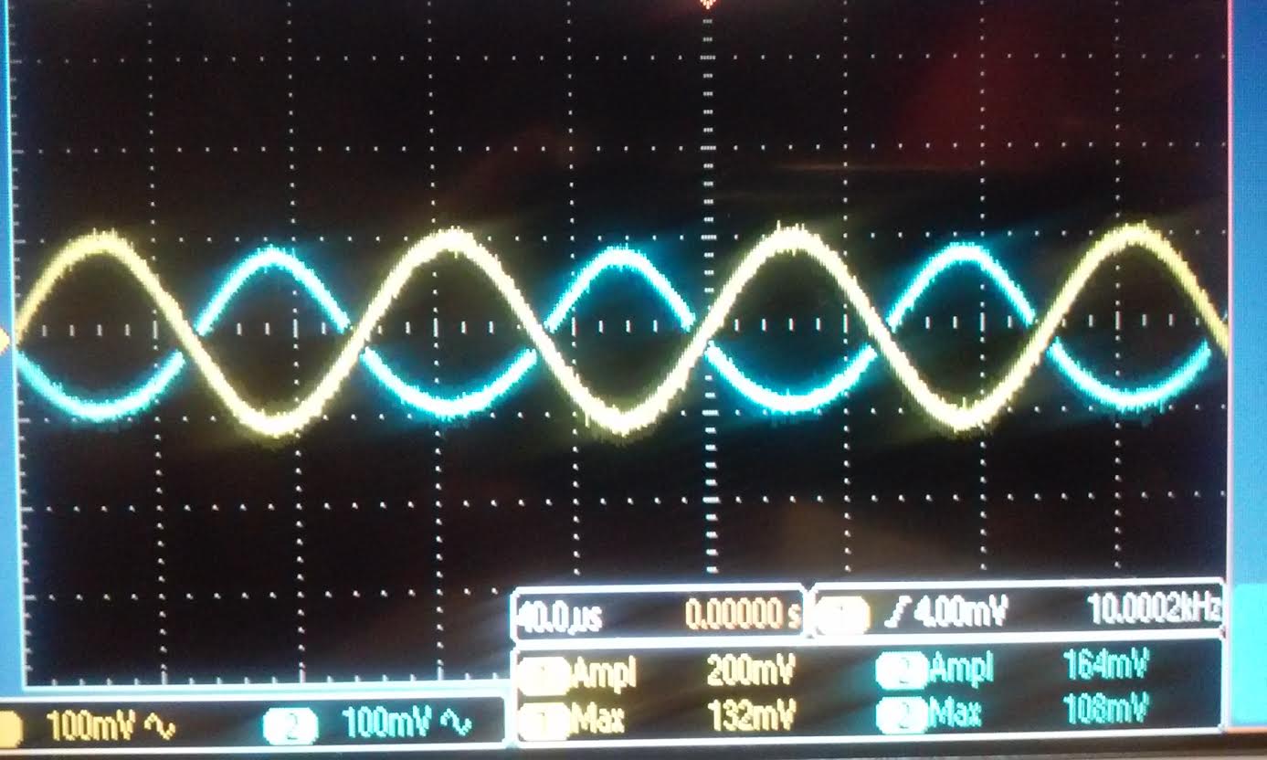
| Rin:
we used Rin=33k for both the Nmos and Pmos our gain for the Nmos is
576mV/200mV = 2.88, and for the Pmos is 160mV/200mV = 0.8 both value is
half of the gain when no resistor was hook up. This indicate that our
output resistance is 33k because it divides the original gain in half
when the 33k resistor was hooked up. |
 |  |
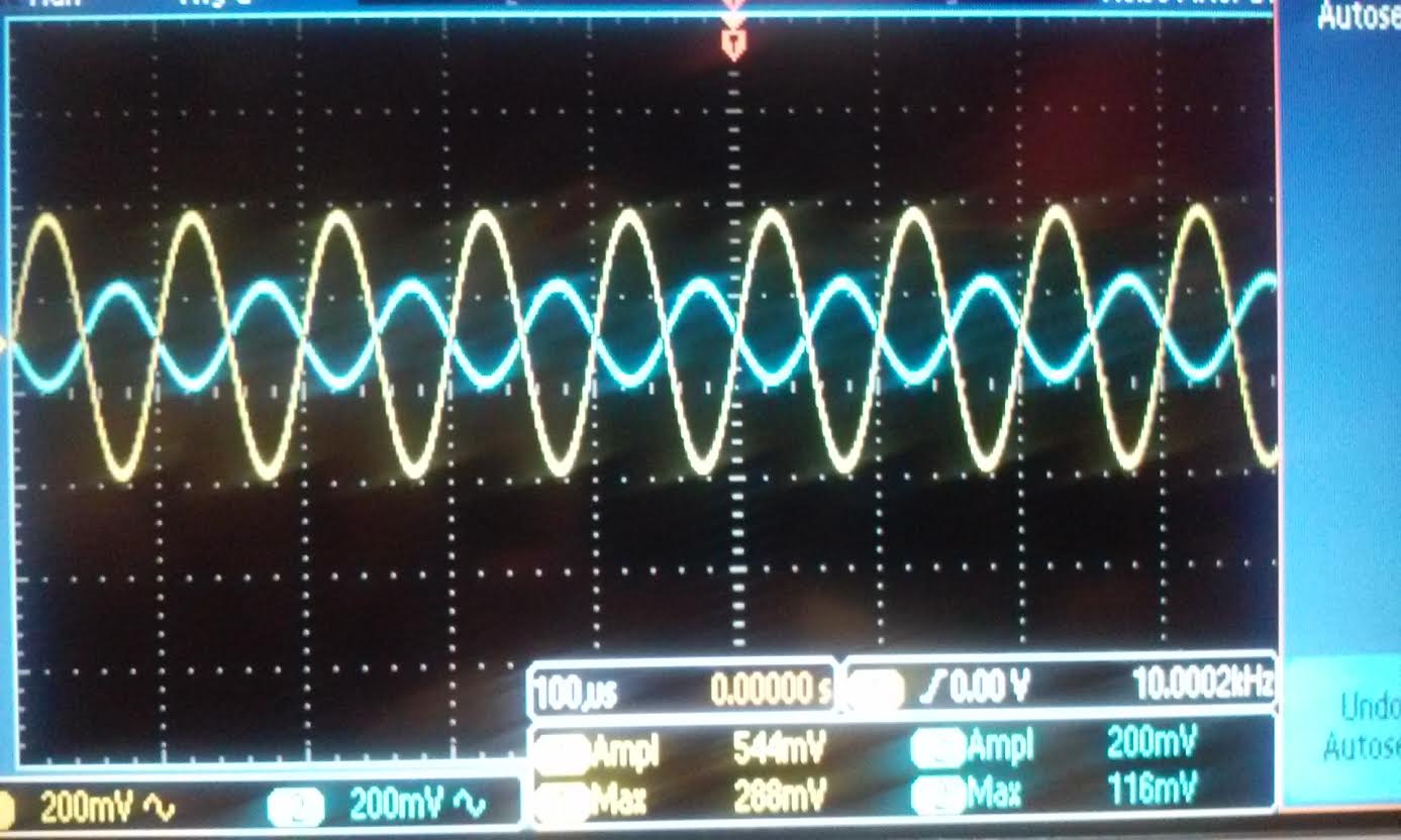
| Rout:
The gain for the Nmos when a 1k resistor is hook up is 544mV/200mV =
2.72, and for the Pmos is 164mV/200mV = 0.82 both of this gain is
roughly half of our original gain. |
 |  |
| Summary: NMOS common-source |
| Hand Calculation | Simulation | Experiment |
| Gain | -6.85 | -6.7 | -5.75 |
| Rin | 33.3k Ohms | 33k Ohms | 33k Ohms |
| Rout | 1k Ohms | 1k Ohms | 1k Ohms |
| Summary: PMOS common-source |
| Hand Calculation | Simulation | Experiment |
| Gain | -5.42 | -5.2 | -1.7 |
| Rin | 33.3k Ohms | 33k Ohms | 33k Ohms |
| Rout | 1k Ohms | 1k Ohms | 1k Ohms |
- Below are two common-gate amplifiers.
- Discuss the operation of these amplifiers in your lab report including both DC and AC operation.
The DC operating point for the NMOS from looking at the
spice error
log and the hand calculation below you can see that gm=18.3mA/V, and
Vout =VDD-id*1k = 3.64V. for the PMOS side the gm is 10.7mA/V and Vout
=id*1k = 384mV, the threshold voltage is also taken from the spice
error log its value is 1.82V for Nmos and -2.88V for Pmos. For AC vdd =
0V, so the operating point Rout and Rin is
limited by the 1k resistor and 50k||100k. Vin and Vout will be limited
by the hand calculations of the gain for AC below.
- Hand calculate the gains and the input/output resistances.
- How does the source resistance, Rsn or Rsp, influence the gain.
Similar to the common-source, if you increase Rs, Rsn or
Rsp then the gain will decrease. - Again compare your hand calculations to simulation and experimental results.
| Simulation of a common-gate amplifier using LTSpice |
| From the transient analysis below we can clearly see that the output of
Voutn = 50mV and Voutp = 70mV, and Vin. The Gain is Vout/Vin so the
gain is 5 for the Pmos and 7 for the Nmos amplifier. This has the same gain as the common-source amplifier This circuit along
with the plot was drafted by Dr. Baker used in prelab. |
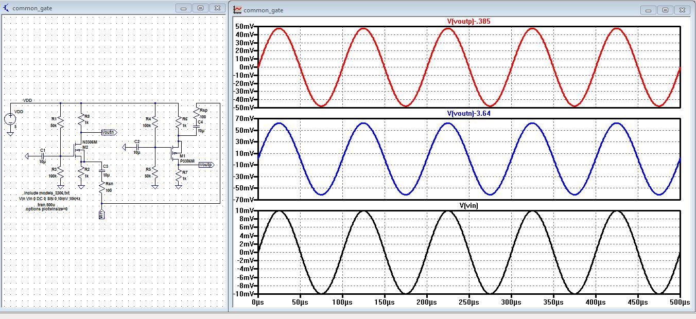 |
| We
can see from the AC analysis below that the gain for Voutn/Vin = 6.2
and Voutp/Vin = 4.8, and both have a phase of -180 degree at 10 kHz. |
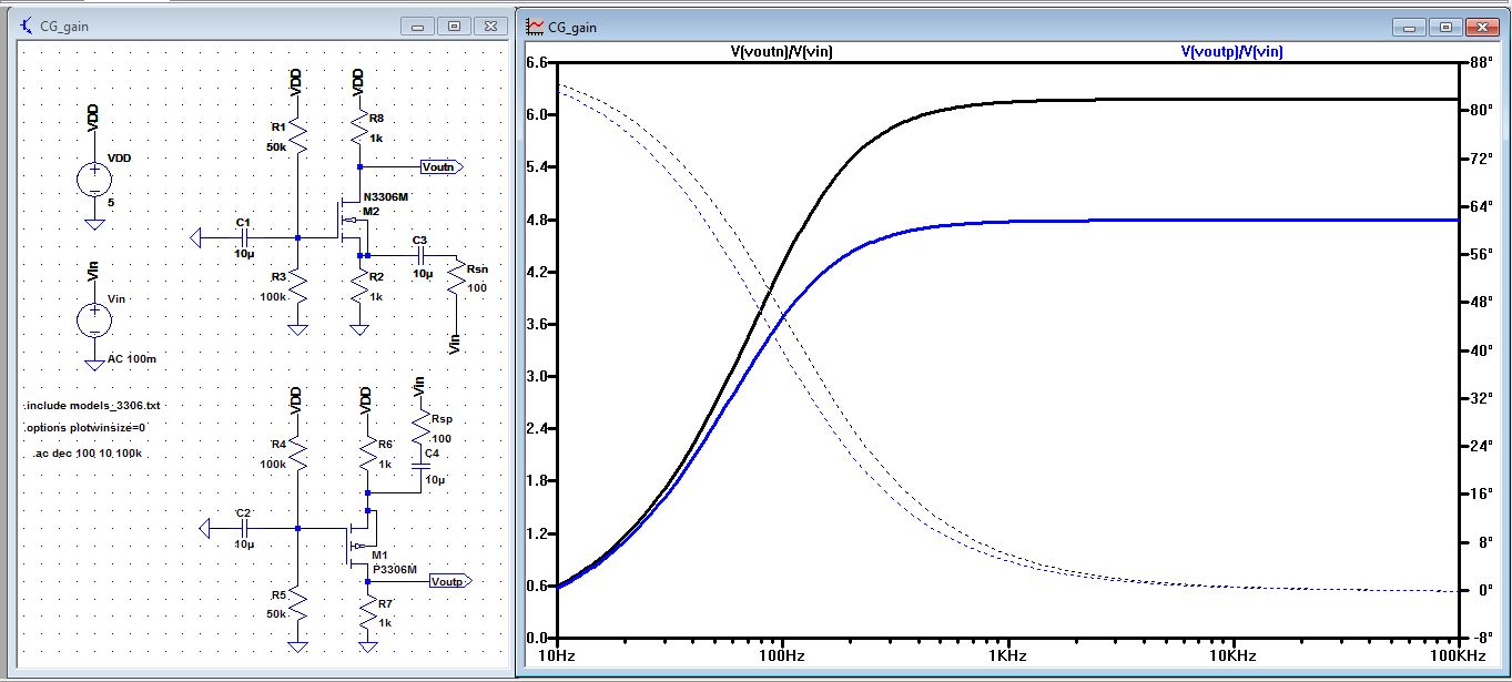 |
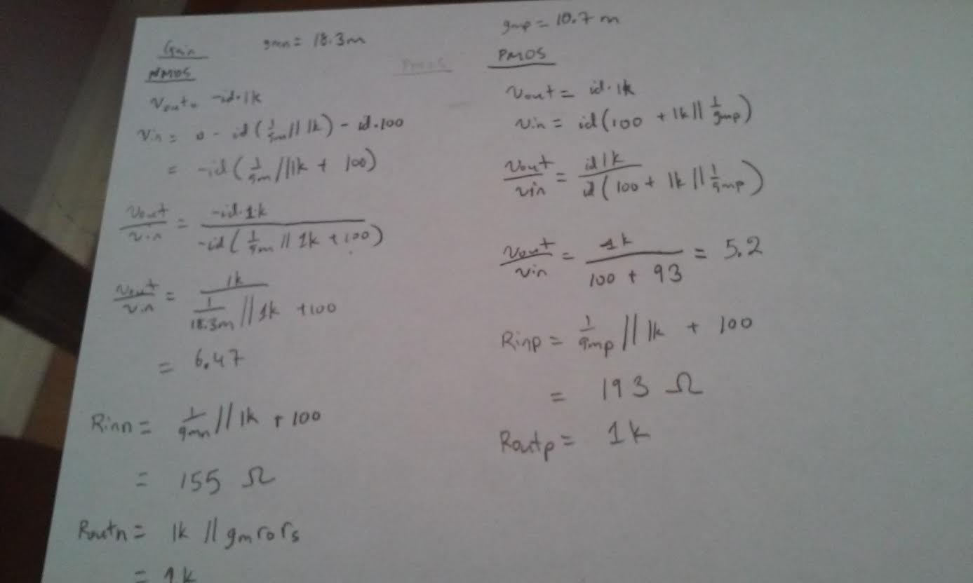
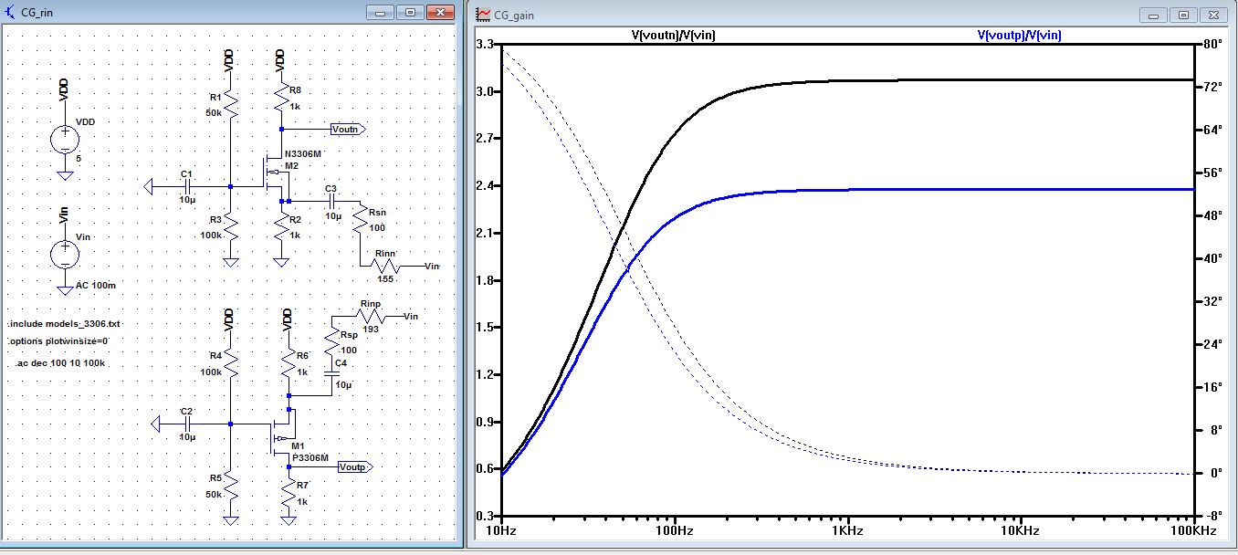
| Rin: From our hand calculation we
got Rinn=155 Ohms, and Rinp=193 Ohms, we use that resistor and hook it
up before the Rsn and Rsp, and our gain is 3.1 for the Voutn/Vin and
2.4 for Voutp/Vin which is half of the original gain without the
divider. |
 |
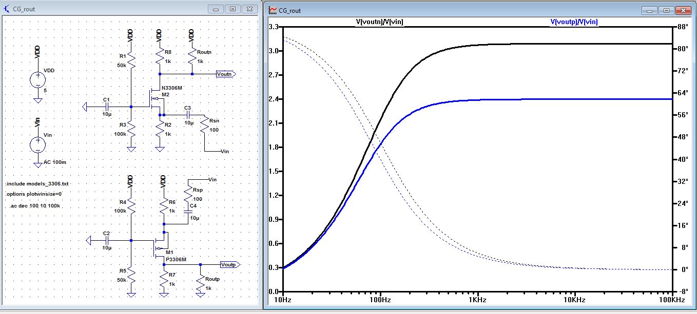
| Rout: we
calculated Rout and it was 1k for both the Pmos and Nmos, so we put a
1k resistor parallel to the R8 and R7 and our gain is 3.1 and 2.4 which
is half of our original Gain, as you can see from the AC analysis
below. |
 |
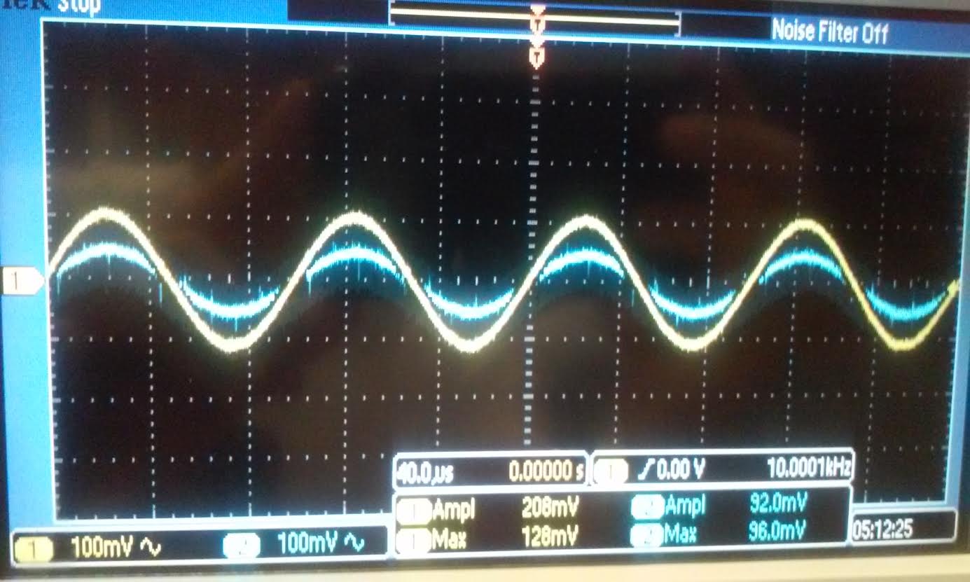
| Experiment of the NMOS and PMOS common-gate amplifier |
| NMOS | PMOS |
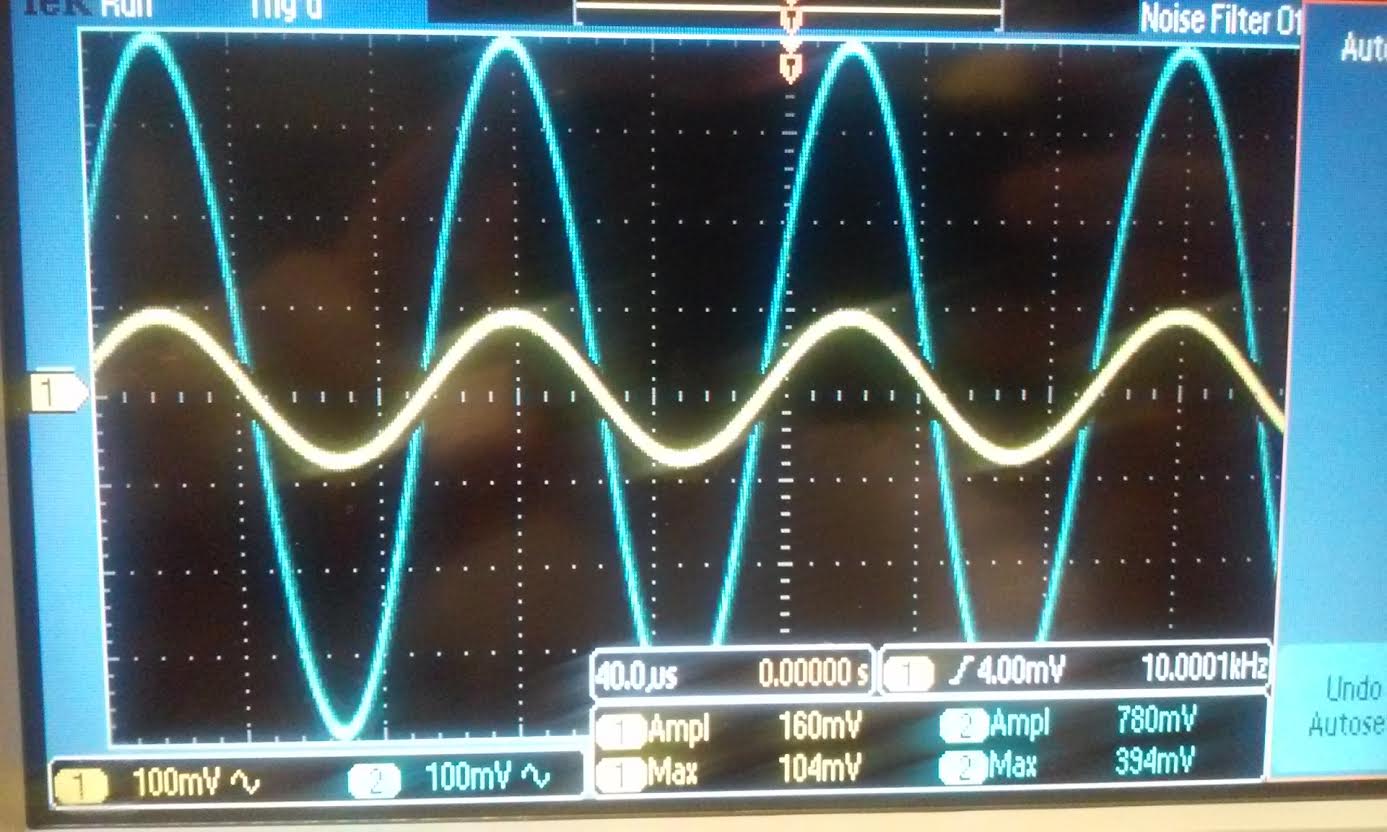
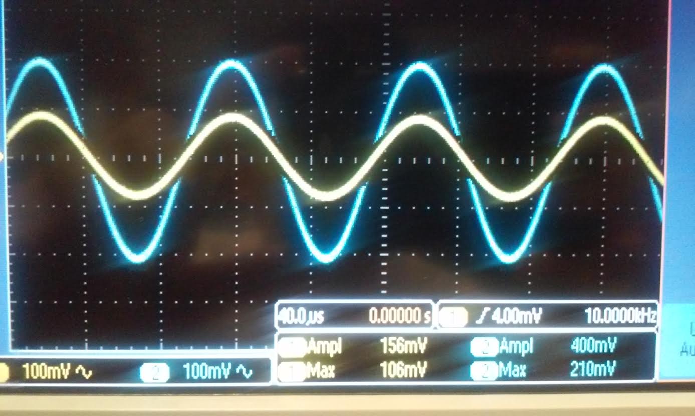
| Gain:
for the Nmos amplifier our experimental gain was 780mV/160mV = 4.9, for
the Pmos the gain is 400mV/156mV = 2.56. Our input was 100mV at 10kHz. In
the data sheet of the ZVP3306A the forward transconductance (gm)
operating point is 60mS while our simulation was only 10.7mA/V. it also
gave the operating condition for Vds = -18V and id=-200mA. Our Vds
operating point was 4.6V and id was only 384uA. |
 |  |
| Rin: For the Nmos we used a 162 Ohms resistor and our gain was 2.5, for
the Pmos we used 620 ohm resistor and our gain was 212mV/192mV = 1.10.
the gains for the Nmos and Pmos is half of our experimental data above.
|
 |  |
| Rout: For
the Nmos we used a 1k resistor and the gain was 476mV/176mV = 2.7. For
the Pmos we used a 1k resistor and our gain was 218mV/176mV = 1.24.
Both of these values is half of our gain of 4.9 for the Nmos and 2.56
for the Pmos. |
 |  |
| Summary: NMOS common-gate |
| Hand Calculation | Simulation | Experiment |
| Gain | 6.47 | 6.2 | 4.9 |
| Rin | 155 Ohms | 155 Ohms | 162 Ohms |
| Rout | 1k Ohms | 1k Ohms | 1k Ohms |
| Summary: PMOS common-gate |
| Hand Calculation | Simulation | Experiment |
| Gain | 5.2 | 4.8 | 2.56 |
| Rin | 193 Ohms | 193 Ohms | 620 Ohms |
| Rout | 1k Ohms | 1k Ohms | 1k Ohms |
- Below is a push-pull amplifier.
- Discuss the operation of this amplifier in your lab report including both DC and AC operation.
For DC analysis since Vout and Vin
are connected in series with the BIG capacitor and BIG resistor so Vout
= Vin, the circuit can self biased because of the BIG resistor thus no
DC current flows in the gate. For AC, Rin = Rout = 100k, assuming the
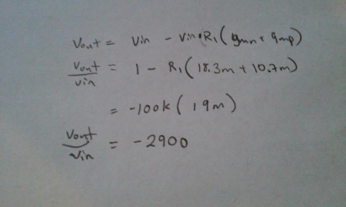
gate resistance is infinitely large. - Hand calculate the gain of this amplifier.
- Do you expect this amplifier to be good at sourcing/sinking current? Why or why not?
Well
depends on the value of VDD, this circuit can source its current to VDD
while it can sink to gnd always. if you think about it the current at
the output will be greater than the current at the input. If you have a
pulse signal coming in then when the pulse is 0 the circuit will source
to VDD and when the pulse is at 1 the circuit will sink the current to
GND. - What happens to the gain if the 100k resistor is replaced with a 510k resistor? Why?
If you increase R1 to 510k then the gain will be 5 times larger
because of the equation of the gain above. - Again compare your hand calculations to simulation and experimental results.
- Note
that the gain of this amplifier is large so the output may saturate at
VDD and Ground. To avoid this saturation you can reduce the AC input
voltage using a voltage divider.
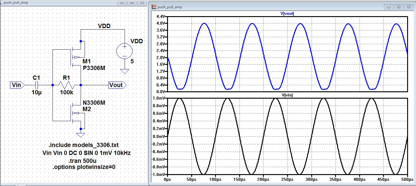
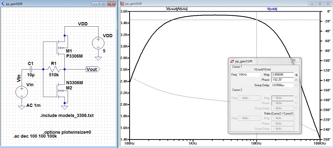
| Simulation of a push-pull amplifier using LTSpice |
| The
schematic below was drafted by Dr. Baker and it shows that the gain is
2V/1mV = 2000 using the transient analysis. where R1=100k |
 |
| Using the AC analysis at 10 kHz you can see that the gain Vout/Vin = 2k, R1 = 100k |
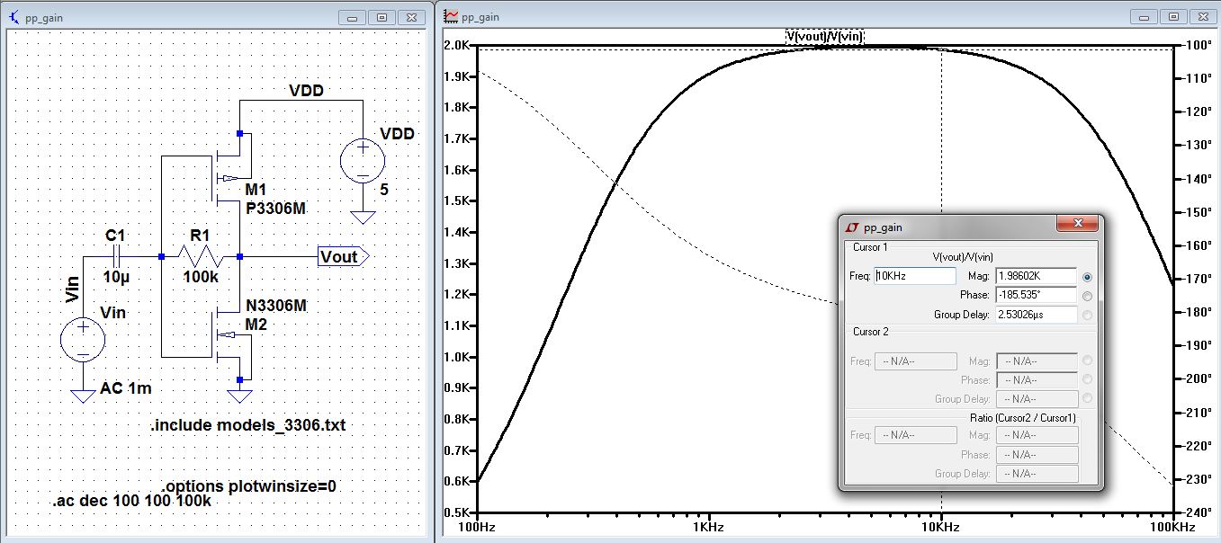 |
| When we put in 510k for R1 we expected it to be 5 times larger than when it was at 100k but the gain is only 3.4k. |
 |
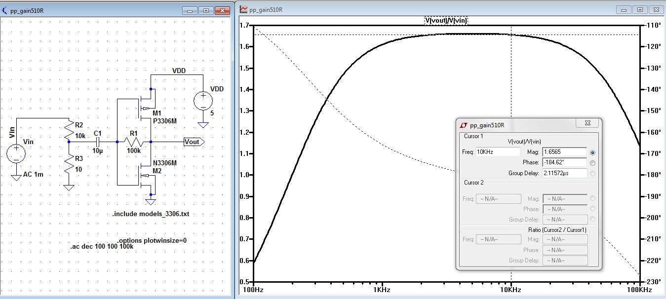
| Voltage divide the input by 1000 with a 10k and 10 ohms resistor, as was expected the gain is now 1.65 instead of 2k. |
 |
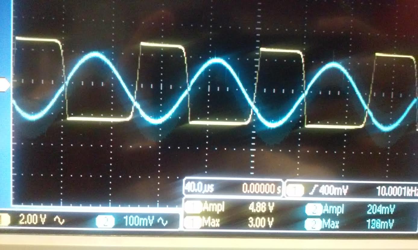
| Experimental: Push-Pull amplifier |
| Gain with no voltage divider. As
you can see from the scope reading the output can only push to GND and
pull to VDD it cannot go beyond VDD. that is why you see a cut-off when
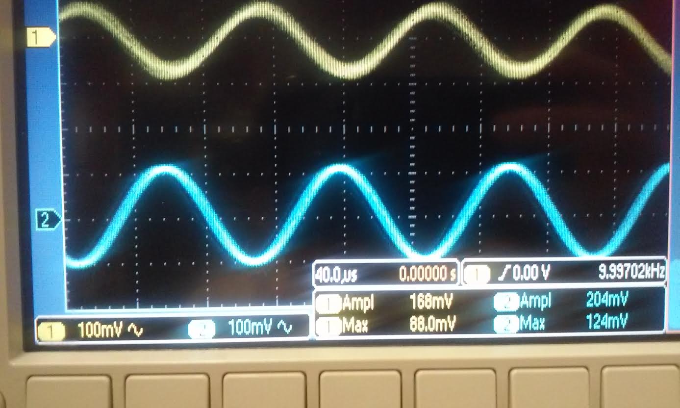
the gain reaches near VDD.SInce its hitting the rail at VDD you cannot see the real gain of the ampligier this way. | Gain with 10k and 10 Ohm voltage divider at Vin. we
hook up the circuit similar to the schematic above and we got 168mV Vin
with a 100mV input. this indicate that our real gain is
1000*168mv=1.68k. |
| 
|
| Summary: Push-Pull amplifier |
| Hand Calculation | Simulation | Experimental |
| Gain | -2.9k | -1.99k | -1.68k |
Conclusion:
Our first experiment involves the source follower amplifier, we found
that both the gain for the Nmos and Pmos was 1, to measure Rin we added
the calculated Rin and put it after the input but before the 10u
capacitor as seen in the schematics. to measure the Rout we used the
calculated value and put it in parallel to the output. For the
Common-source amplifier the calculated gain for the Nmos was 7, the
gain for the Pmos was 5. Both had a phase shift of -180 degree which
indicate that the gain is negative for the experiment and
and simulation result. For the Common-gate amplifier the gain was the
same but there was no phase shift. for the push-pull amplifier the gain
was 2900 for the calculated values and 2k for the simulation, the gain
was so high that it rail from GND to VDD, in order to fix this we had
to voltage divide the input with a 10k and 10 ohms resistors and the
experiment gave us a 1.68k gain with a 180 degree phase difference.
Return to EE420L front page