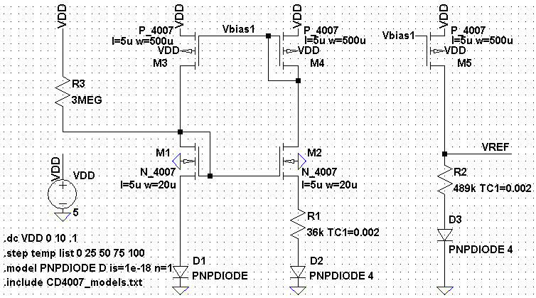
Figure 1a.
In this experiment, a bandgap reference is designed and tested on a breadboard using CD4007 CMOS arrays. The simulation is performed in LTSpice using the Level=1 model specified in CD4007_models.txt. The widths and lengths of the devices in the simulation are chosen to match those specified in the CD4007.txt models provided by Dr. Garia-Inza of the University of Buenos Aires.
Background
A
bandgap reference (BGR) generates a voltage (VREF) that does not vary much with
temperature or with supply voltage (VDD). Toward the goal of temperature
invariance, a BGR can be designed to have two stages, the first having PTAT
behavior and the second negating that behavior. Toward the goal of supply
voltage invariance, the BGR can be designed to have high output impedance,
either by cascoding the devices at the output (in long-channel processes) or by
regulating their drain voltage with an amplifier (in short-channel processes).
A voltage is PTAT (proportional to absolute temperature) if it increases with increasing temperature and CTAT (complementary to absolute temperature) if it decreases with increasing temperature. The PTAT behavior of a reference can be negated when combined with a circuit that exhibits CTAT behavior. This method is used to design the BGR in this experiment.
The PTAT
Component
For the following discussion, refer to the branches containing M1 and M2 in Figure 1a.
Figure 1a. |
Using
the relationship between the voltage across a diode and its forward current,
equations for the voltages across D1 and D2 can be obtained as:

Note that
ID2 is scaled down by a factor of uppercase K (not to be confused with
Boltzmann’s constant k), which represents the number of diodes connected in
parallel. This parallel arrangement is necessary in order to drop the same
voltage below M1 and M2 when constructing the circuit on a breadboard using
diodes of matching sizes. That is, VD2 must be smaller than VD1, and in order
to achieve this, the current from M2 must be split between K diodes. The
difference between VD2 and VD1 is then dropped across the resistor.
The
gate-drain connection sets the VSG and VSD of the PMOS in each branch to be
equal, forcing the same current to flow in each branch and thus the same
current to flow in D1 and D2. Knowing this, an equation can be obtained for the
resistor in the PTAT reference by substituting the equations for VD1 and VD2
into Ohm’s law:

To avoid cluttering the breadboard in this experiment, a relatively small value of K = 4 was chosen. For the arbitrarily chosen reference current of 1 μA, the above equation yields R = 36 kΩ.
Negating
the PTAT Behavior
From the
derived equation for R, the reference current that flows in each branch can be
obtained as:

Performing
KVL and substituting the above expression for the current, an equation for VREF
can be obtained as:

Note
that VREF depends on two terms that behave differently with temperature.
Firstly, VD3 decreases with temperature, according to the relationship between
a diode’s forward current and the voltage across it. Secondly, VT increases
with temperature, as described by kT/q. These two opposing temperature
behaviors negate one another, causing VREF to become independent of temperature
if the appropriate value of L is chosen.
To
choose a value of L for which VREF does not vary with temperature, an equation
is needed which describes the temperature-dependence of VREF. This equation can
be obtained by taking its partial derivative with respect to temperature:
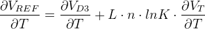
The
change in VD3 with respect to temperature can be obtained as –1.6 mV/°
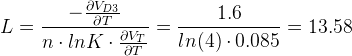
Using
the above value of L = 13.58, along with K = 4, VT = 26 mV, n = 1, and VD3 as
obtained from the equation for VD2, the value of VREF can be estimated as:

The
simulation produces a separate curve of VREF with respect to VDD for each temperature
from 0 °
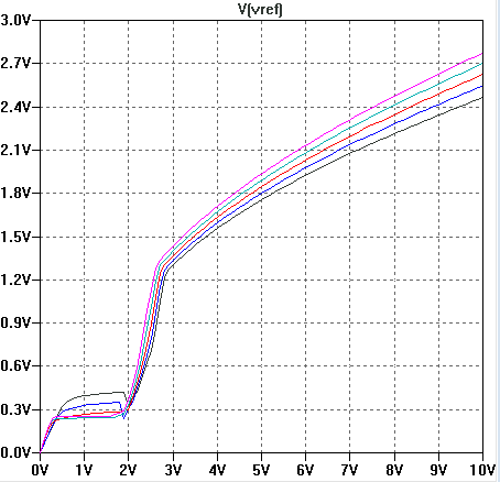 Figure 1b. |
The temperature coefficient (tempco) of VREF can be obtained as the ratio of its change with temperature to its expected value (as estimated for VDD = 3 V in the Negating the PTAT Behavior discussion):

Its
change with respect to temperature is estimated from the simulation
(Figure 1b) as the difference between its value at 100 °
The variation
in VREF with respect to VDD is a consequence of the finite impedance seen at
the drain of M2 and M4. Cascoding either the PMOS or the NMOS would increase
the total impedance seen at this node. However, cascoding only one of the devices
is not sufficient to prevent the variations in VREF.
Cascoding
only the PMOS would cause the current in each branch to match, but the currents
would not remain constant because the drain voltages of M1 and M2 would be free
to move with VDD. Cascoding only the NMOS would cause their drain-source
voltages to remain constant, but the branch currents would be unequal due to
the drain-source voltages of the PMOS being unequal. For these reasons, if any
cascoding is used, both PMOS and NMOS must be cascoded.
A
disadvantage of the cascode, however, is an increase in the minimum VDD
required for the devices to operate in saturation. This consequence is
insignificant in long-channel processes, in which the threshold voltages are a small
percentage of VDD, but in short-channel processes, the threshold voltages are
relatively large, and the required gate-source voltages may add up to a total
greater than VDD. For this reason, the cascoding method of reducing sensitivity
to VDD is reserved for long-channel devices, such as those used in this
experiment.
As seen
in the Performance discussion, the
devices are not cascoded in the BGR tested in the experiment. Thus, the
measurements show that VREF depends on VDD noticeably.
Start-Up
Two
possible states of operation exist for the reference, one of which is the
conducting state described above. The other state is one in which no current
flows in the branches. In this zero-current state, the gates of M1 and M2 are
at ground potential. To force the circuit to assume the conducting state, a
large resistor, such as the 3-MΩ resistor used in this experiment, can be
connected from the supply voltage to the gate of M1. The potential difference
between the supply voltage and M1’s gate causes a current to leak into M1, at
which point, M1 promptly activates and mirrors its current into the other branch,
and the circuit has then assumed the conducting state.
Performance
Measurements for VREF were taken for VDD increasing from 1 V to 10 V in increments of 1 V (Figure 2a). When the values for VREF with respect to VDD are plotted in Microsoft Excel (Figure 2b), the resulting curve is similar to that obtained from the simulation (Figure 1b). In both curves, the references begins to generate the expected VREF at about VDD = 3 V.
The
measured VREF reaches beyond 3 V when VDD reaches its peak, a value higher than
that reached in the simulation, indicating that the actual impedance at the
drain of M2 and M4 is smaller than that specified by the simulation model.
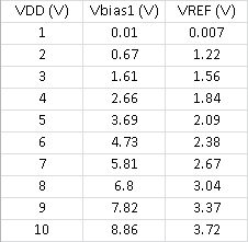 Figure 2a. |
 Figure 2b. |