ECE 421L - Lab 9

John Huang

Huangj19@unlv.nevada.edu

Spring 2015


For this lab we will be using the CD4007 CMOS transistor array.

The models we used for all our simulations can be found here.


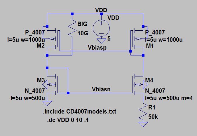
We will build our BMR design and characterize it as we did in the prelab.

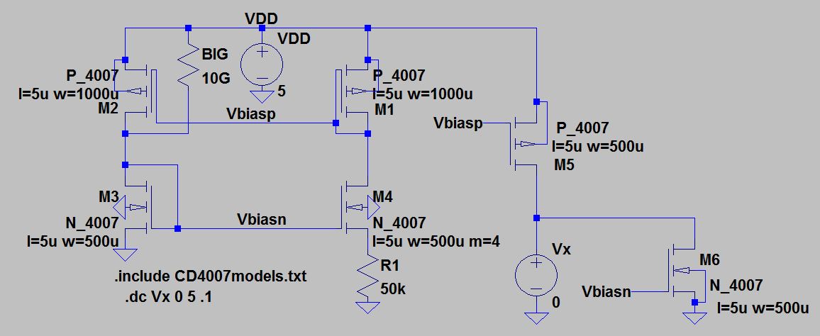
We used this design from our prelab for our BMR.

http://cmosedu.com/jbaker/courses/ee420L/s15/students/huangj19/lab9/1.JPG


As specified from our prelab, we will be using a large resistor (10G ohms) for the start-up current, this is done by the leakage currrent going through the resistor.

We had to double the widths of our PMOS devices because of the different in the KPP and KPN values in our models.

We will also be using the W/L of 500um/5um from the previous lab.

We picked the resistor to be 50k so that we get the expected gm of 20uA/V since gm = 1/R.


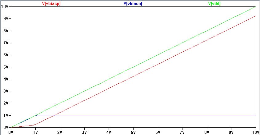
Simulation our above design gives us our desires results.

http://cmosedu.com/jbaker/courses/ee420L/s15/students/huangj19/lab9/2.JPG


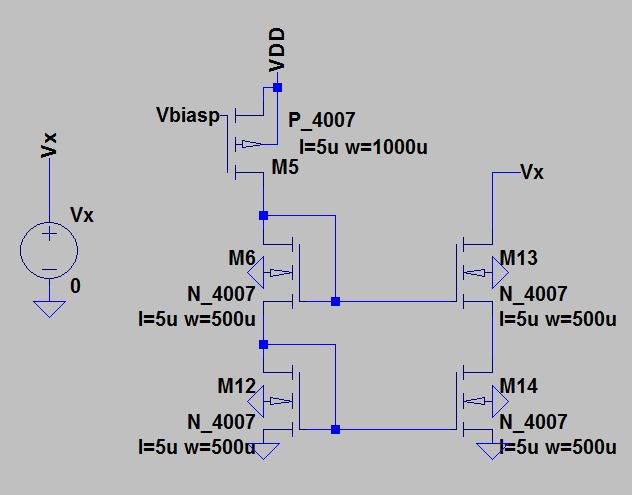
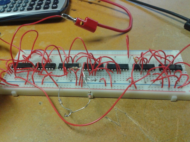
Putting the BMR together we had to use 7 CD4007 transistors.

http://cmosedu.com/jbaker/courses/ee420L/s15/students/huangj19/lab9/3.jpg


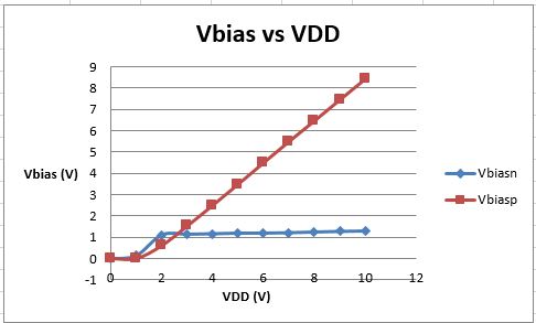
Using this we then measured the Vbiasn and Vbiasp voltages while we adjusted our VDD voltage from 0 to 10V.

http://cmosedu.com/jbaker/courses/ee420L/s15/students/huangj19/lab9/4.JPG

http://cmosedu.com/jbaker/courses/ee420L/s15/students/huangj19/lab9/5.JPG


In order to show that a large capacitance across the resistor becomes unstable we did the following experiment:

We shunt the 50k resistor with a 1000uF capacitor and put a 0 to 1V (VDD) square pulse signal as an input.

The following experiment resulted in the following graph
http://cmosedu.com/jbaker/courses/ee420L/s15/students/huangj19/lab9/6.jpg


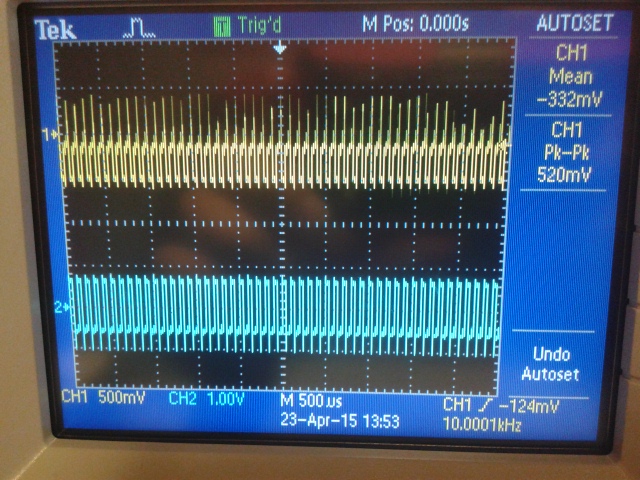
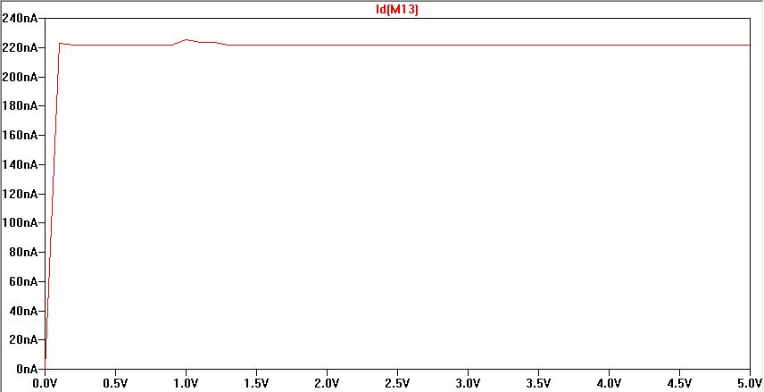
Using our BMR to bias we created a NMOS and PMOS current mirror

http://cmosedu.com/jbaker/courses/ee420L/s15/students/huangj19/lab9/7.JPG


Measuring the current through each current mirror as the voltage across the mirror changes.

http://cmosedu.com/jbaker/courses/ee420L/s15/students/huangj19/lab9/8.JPG


Then graphing them we get the following curves.

http://cmosedu.com/jbaker/courses/ee420L/s15/students/huangj19/lab9/9.JPG    http://cmosedu.com/jbaker/courses/ee420L/s15/students/huangj19/lab9/10.JPG


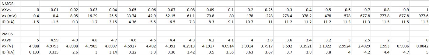
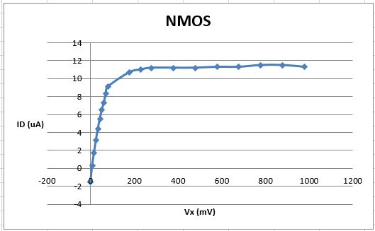
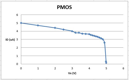
From our simulation we can see that the curves are a close representation of the simulation curves.

Where ID(M5) is the PMOS and ID(M6) is the NMOS.

http://cmosedu.com/jbaker/courses/ee420L/s15/students/huangj19/lab9/11.JPG


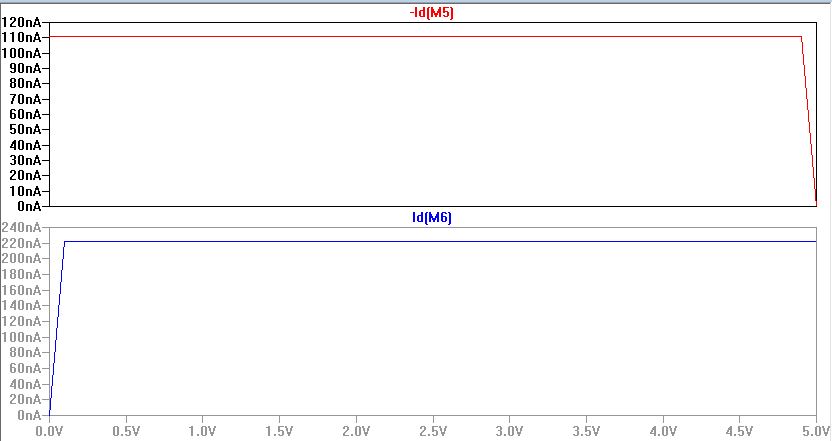
For the NMOS the voltage only went up to 1.2 volts because the current after that point stayed the same till 5V.

For the PMOS the voltage was increasingly steadily even up to 5V therefore we kept the small increasing amounts of current for our graphs.


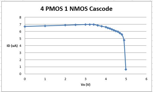
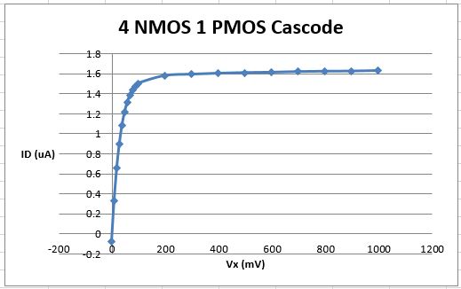
Now using these two devices we are to drive two gate-drain connected transistors.

NMOS current mirror driving two PMOS gate-drain connected devices (cascode)

http://cmosedu.com/jbaker/courses/ee420L/s15/students/huangj19/lab9/12.JPG


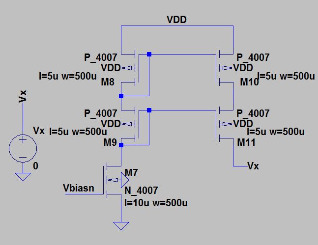
Measuring the current as we sweep VDD we get the following.

http://cmosedu.com/jbaker/courses/ee420L/s15/students/huangj19/lab9/13.JPG

http://cmosedu.com/jbaker/courses/ee420L/s15/students/huangj19/lab9/14.JPG

 
Comparing this to our simulation we can see that the curve is the same however the values of ID are a bit off
http://cmosedu.com/jbaker/courses/ee420L/s15/students/huangj19/lab9/15.JPG 
 
PMOS current mirror driving two NMOS gate-drain connected devices (cascode)
http://cmosedu.com/jbaker/courses/ee420L/s15/students/huangj19/lab9/16.JPG
 
Measurign the current as we sweep VDD we get the following.
http://cmosedu.com/jbaker/courses/ee420L/s15/students/huangj19/lab9/17.JPG
http://cmosedu.com/jbaker/courses/ee420L/s15/students/huangj19/lab9/18.JPG
 
Comparing this to our simulation we can see the same thing as the previous experiment, that our curve is relatively the same however the magnitude of ID is off
http://cmosedu.com/jbaker/courses/ee420L/s15/students/huangj19/lab9/19.JPG
 
Conclusion:
From our design of our BMR we were able to experimentally get correct response in terms of the curve shape, however our actual current measured was higher than the simulations.
Our equiptment in our lab that we used also does not measure past 100nA, which provides a problem when our simulation shows results much smaller than that.
Differentiation of our results based on the current can be affected by current leakage from our transistors and resistance from our wires when we make measurements of such small magnitude.
 
Backup:
Make sure you back up your whole CMOSedu folder with all your labs by compressing the folder and sending it to yourself through email.
http://cmosedu.com/jbaker/courses/ee420L/s15/students/huangj19/lab9/20.JPG


Return to my lab reports


Return to student lab reports


Return to ee420L webpage