ECE 421L - Lab 8
For all our measurements we only measured ID with VGS or VDS individually because we did not know how to sweep them on the oscilloscope.
We recorded the data and used excel to plot our ID v. VGS/VDS/VSG/VSD curves.
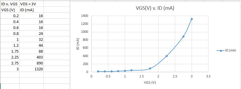
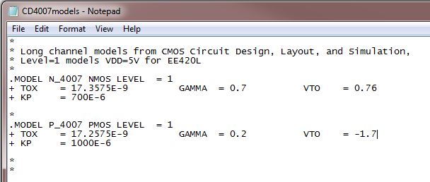
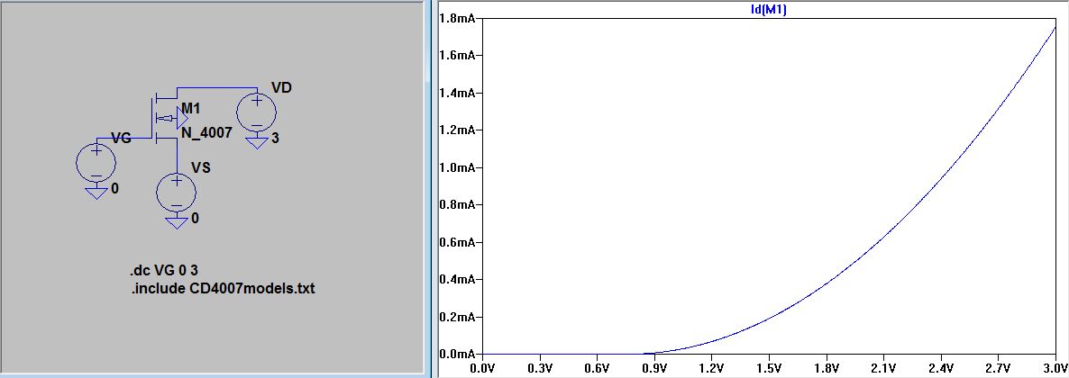
1. ID v. VGS (0 < VGS < 3V) with VDS = 3V
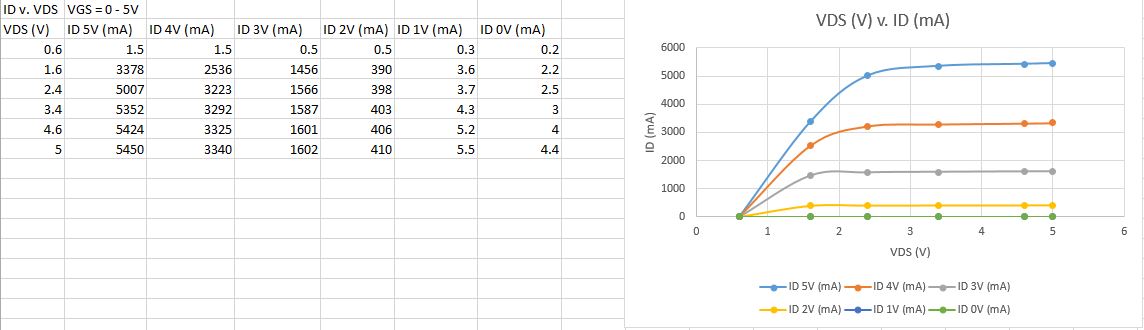
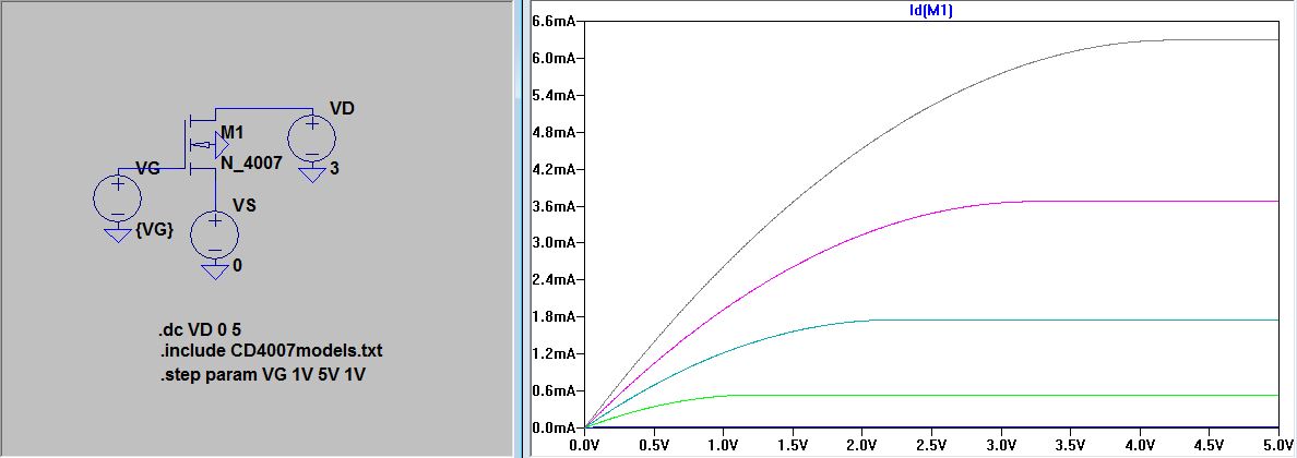
2. ID v. VDS (0 < VDS < 5V) for VGS varying from 1 to 5V in 1V steps
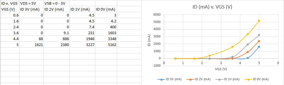
3. ID v. VGS (0 < VGS < 5V) with VDS = 5V for VSB vraying from 0 to 3V in 1V steps
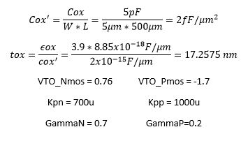
With this data we created a level = 1 MOSFET model with only parameters of VTO, GAMMA, KP and TOX.
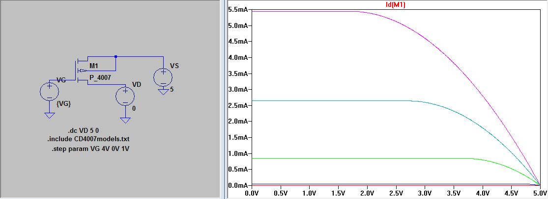
ID v. VDS (0 < VDS < 5V) for VGS varying from 1 to 5V in 1V steps
ID v. VGS (0 < VGS < 5V) with VDS = 5V for VSB varying from 0 to 3V in 1V steps
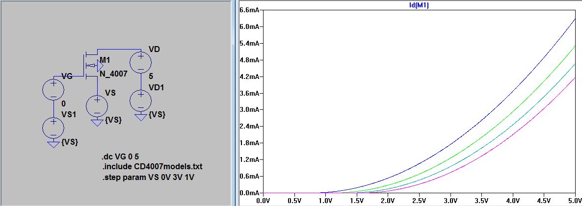
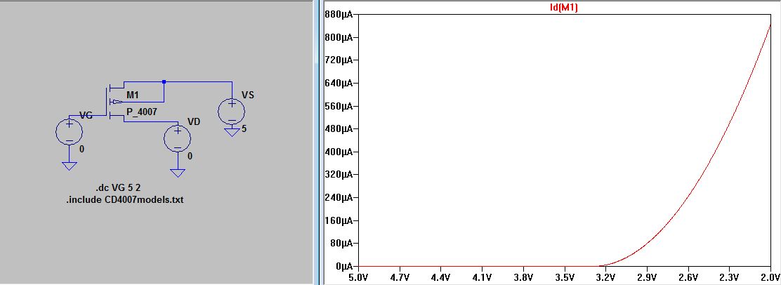
As you can see our simulations match our experimental simulated graphs very closely.
Now we repeat these steps for the PMOS placing VDS, VGS, VSB with VSD, VSG, VBS respectively.
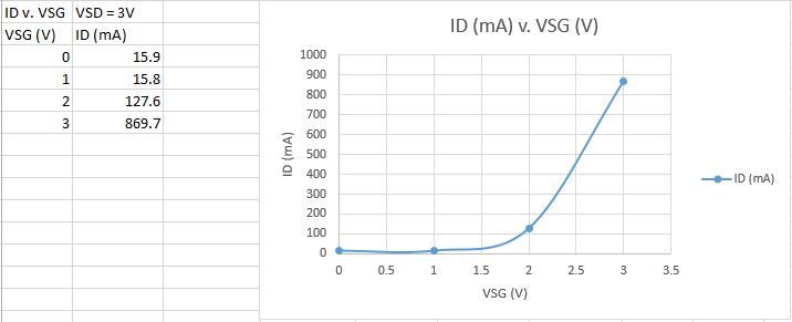
4. ID v. VSG (0 < VSG< 3V) with VSD = 3V
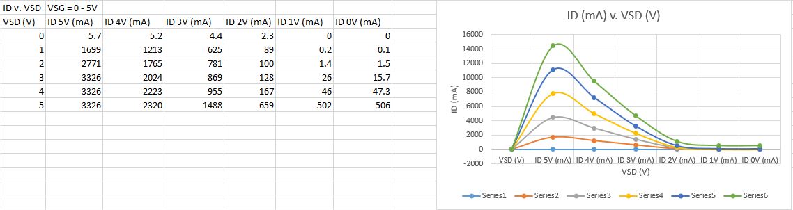
5. ID v. VSD (0 < VSD < 5V) for VSG varying from 1 to 5V in 1V steps
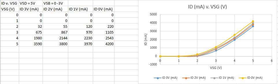
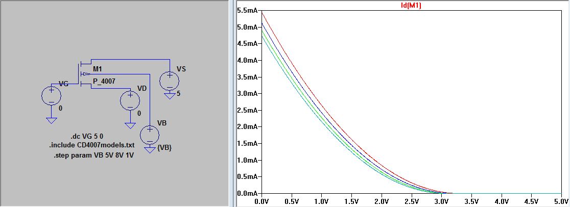
6. ID v. VSG (0 < VSG < 5V) with VSD = 5V for varying VBS from 0 to 3V in 1V steps
Now we can compare these experimental simulated graphs with our simulations
ID v. VSG (0 < VSG< 3V) with VSD = 3V
ID v. VSD (0 < VSD < 5V) for VSG varying from 1 to 5V in 1V steps
ID v. VSG (0 < VSG < 5V) with VSD = 5V for varying VBS from 0 to 3V in 1V st
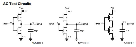
Experimentally, similiar to what is seen on the datasheet (AC test circuits seen on page 3 of the datasheet), measure the delay of an inverter using these devices.
Remember the loading of the scope probe is around 15pF and there is other stray capacitance, say another 10pF.
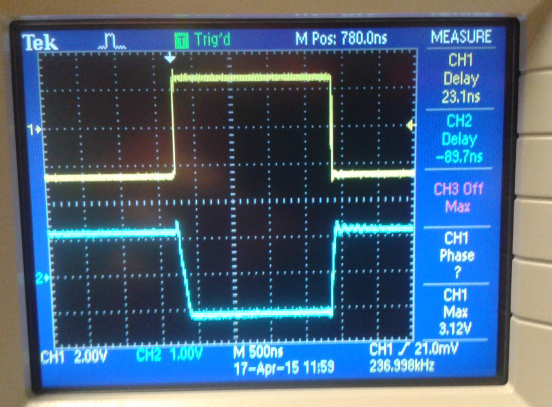
Using your model simulate the delay of the inverter and compare to measured results.
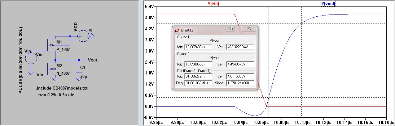
We measured a total time delay of 23.1ns while our simulation showed around 31.4ns.
This is very close as we are not measuring the time delay at exactly the same spot.
Conclusion:
From this experiment we can see how we are able to see how the CD4007 CMOS transistor array behaves.
We can compare how the drain current of each mosfet behaves with varying voltages of VGS, VDS, VSB, VSG, VSD, VBS.
From the graphs we can see when the mosfets start to turn on and the points at when it starts to saturate.
We are also able to make our own spice models from these experiment data results in order to use them in LTSpice.
We were able to compare our spice models by measuring the time delay of the inverter in the CD4007 using the AC test circuit inverter example.
Back up:
Make sure you back up your whole CMOSedu folder with all your labs by compressing the folder and sending it to yourself through email.