ECE 421L - Lab 6
Lab Description:
Lab 6 is to learn about single-stage transistor amplifiers. We will be looking at 4 different types of single stage amplifiers.
The source follower (common-drain), common-source, common-gate and push-pull amplifier.
All experiments were run at 10kHz to ensure that our capacitor have negligible impedance.
All experiments that required capcactiors were done using electrolitic capacitors with the positive terminal connected to the higher potential and the negative potential connected to the lower potential.
This means that the positive side is usually connected to the gate of the mosfet while the negative side is connected to the function generation (vin).
This lab will utilize the ZVN3306A and ZVP3306A mosfets.
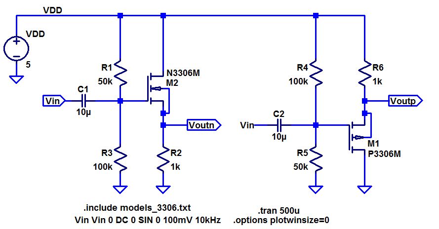
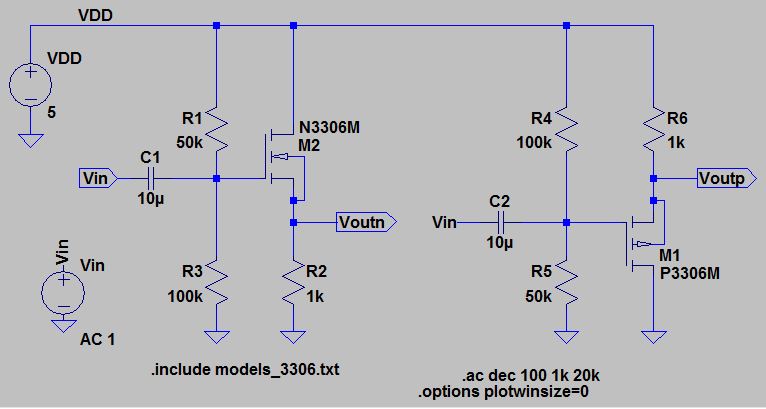
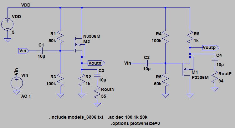
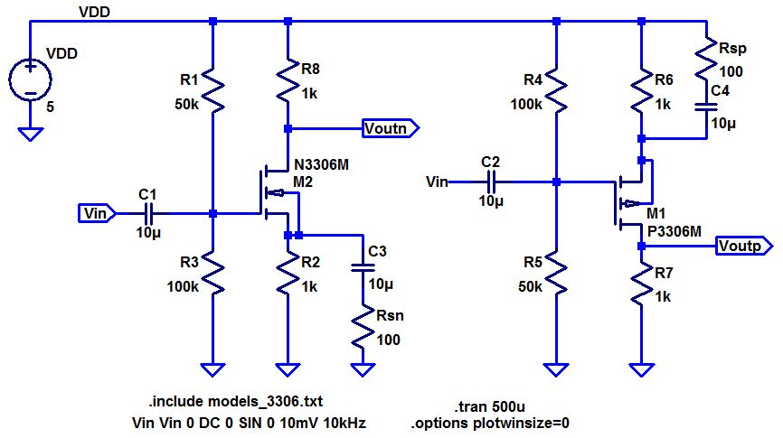
Below is the schematic for our NMOS and PMOS source follower/common-drain amplifier.
We can tell that this design is a common-drain amplifier because both the inputs are coming into the gate of the mosfet and out the source of the mosfet.
The remaining terminal is the drain which makes it a common-drain amplifier.
DC simulation:
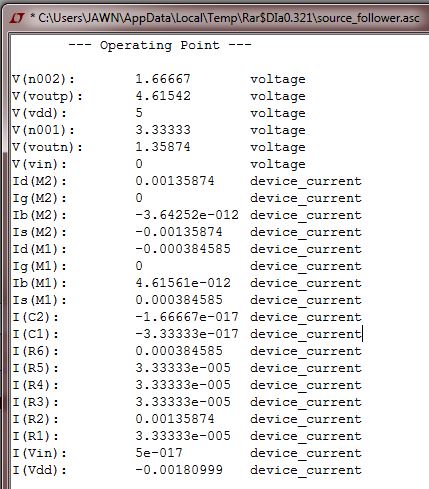
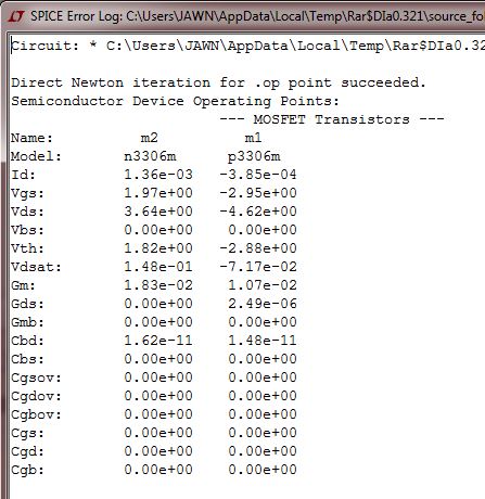
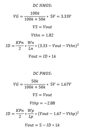
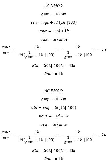
DC hand calculations:
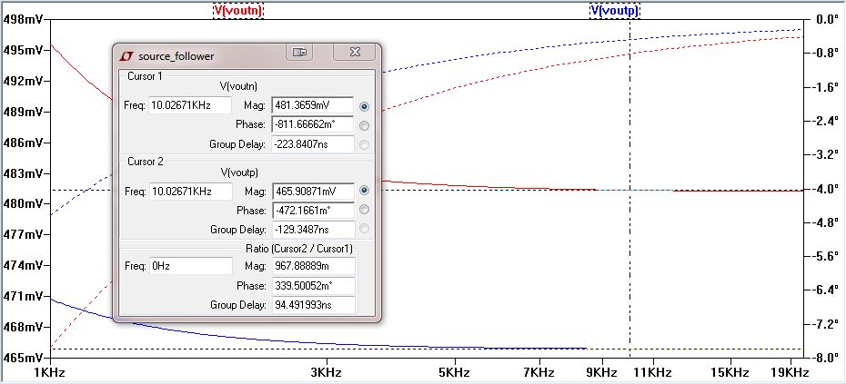
AC simulation:
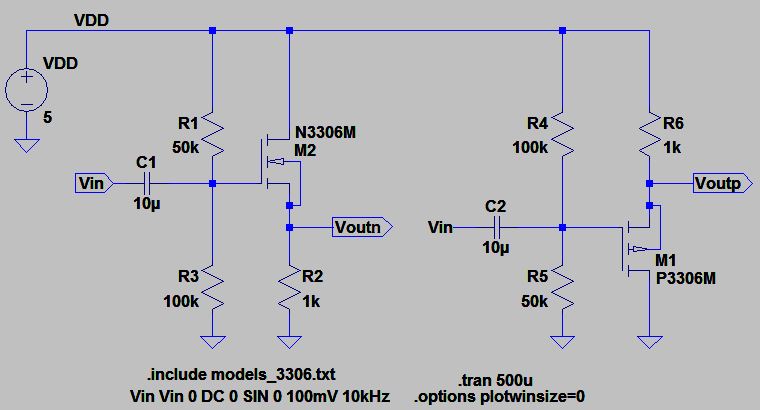
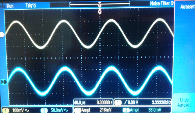
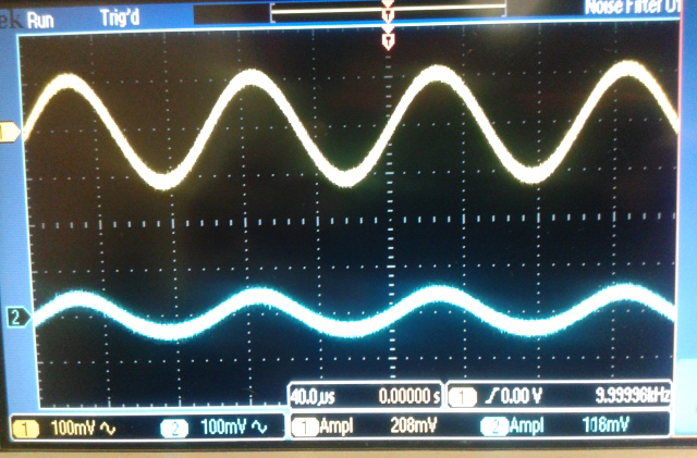
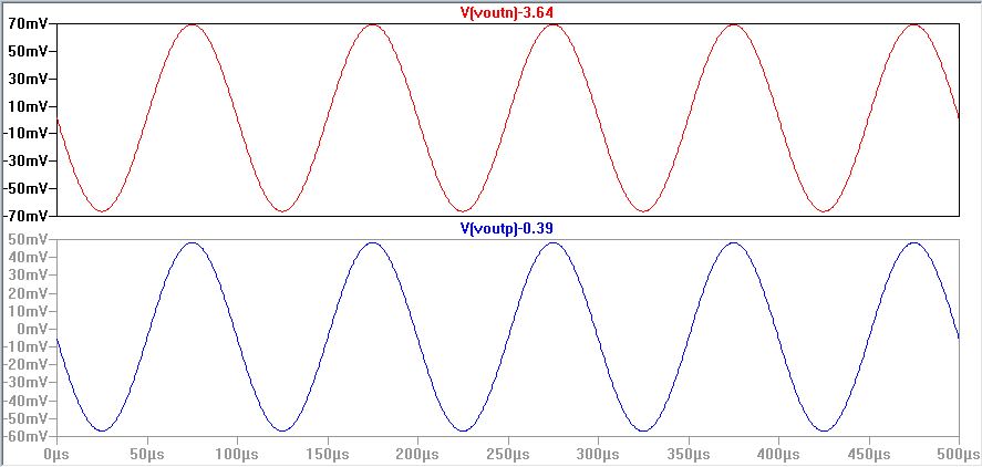
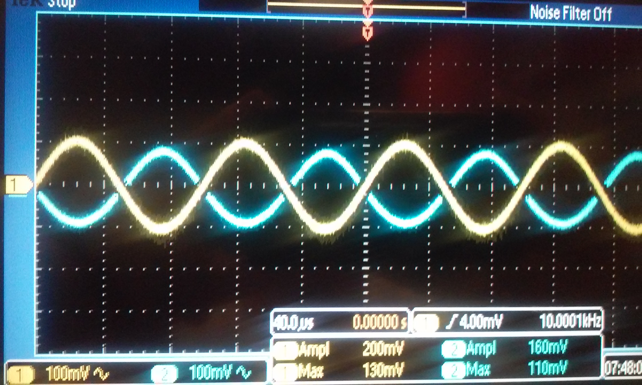
We can see that the gain for the NMOS and PMOS is 1 since Vin is set at 100mV.
AC hand calculations:
Experiment:
| NMOS | PMOS |
 | 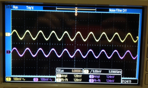 |
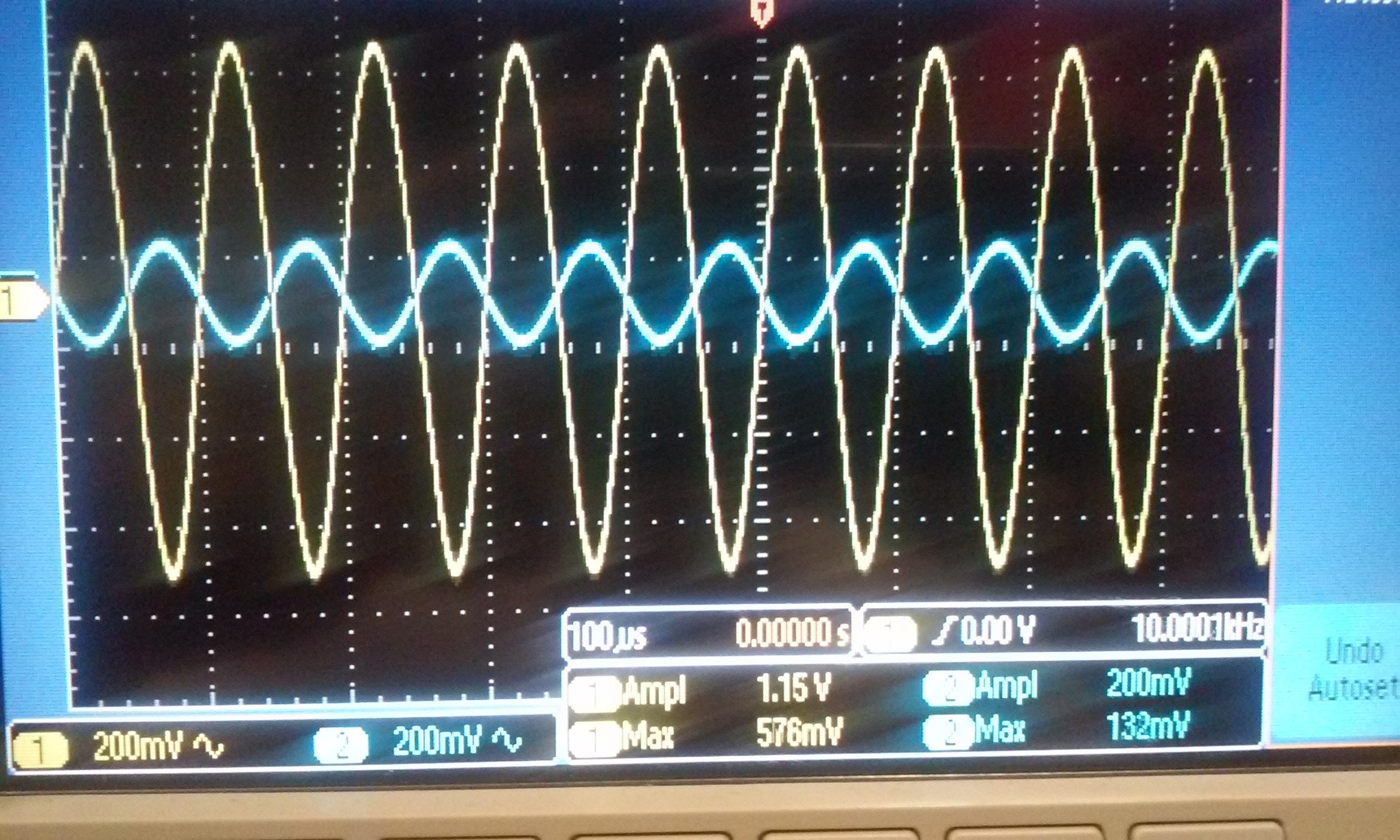
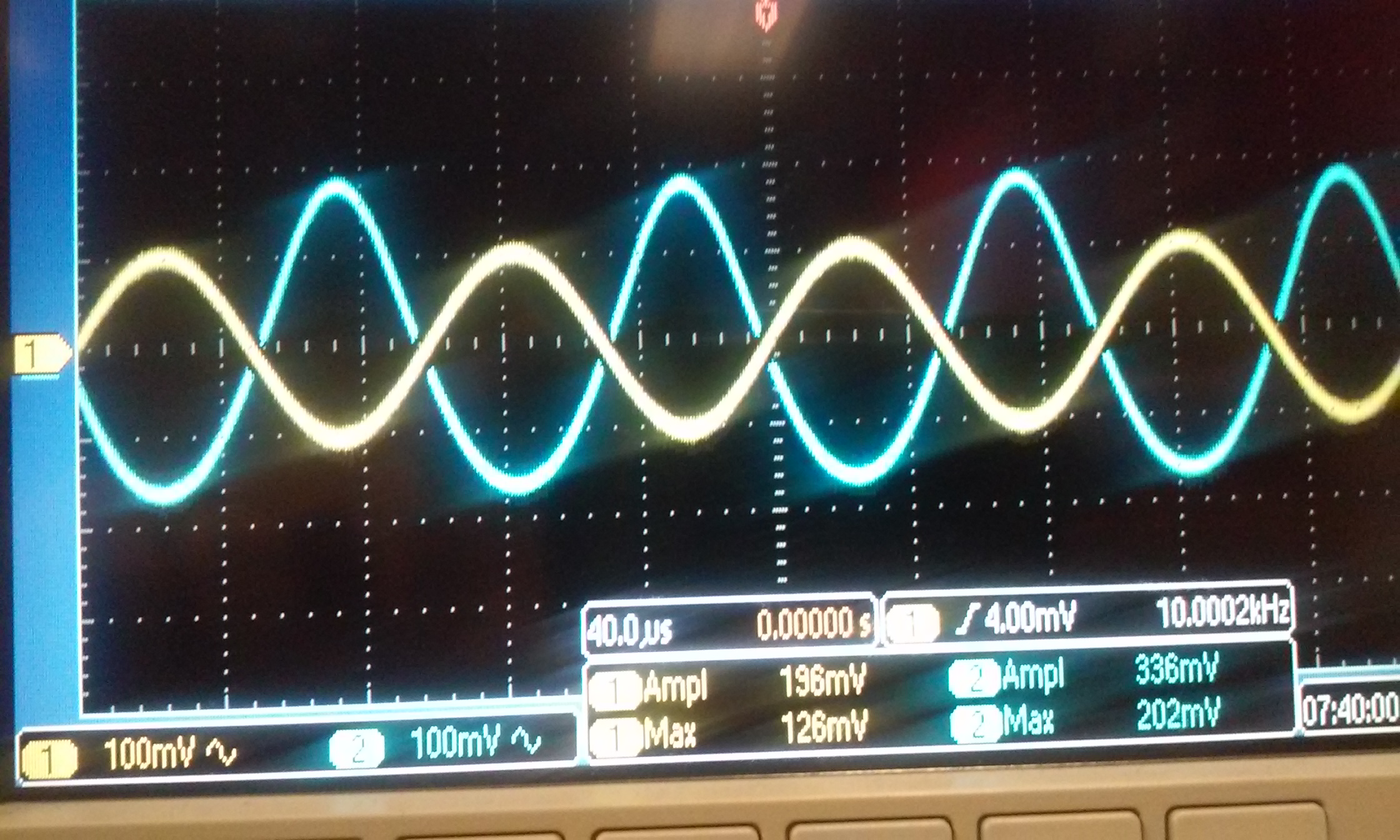
We can see that the gain of both NMOS and PMOS are approximately 0.9-1.
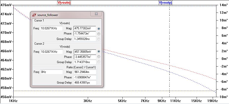
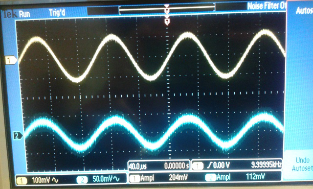
If we use an AC analysis we can again verify the gain of the source follower.
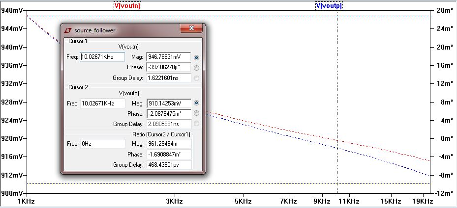
And from our simulations this proves to be almost true being that the gain of the NMOS is 0.947 and PMOS is 0.910.
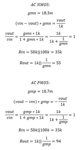
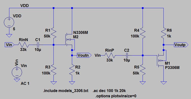
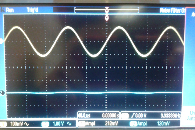
Input resistance:
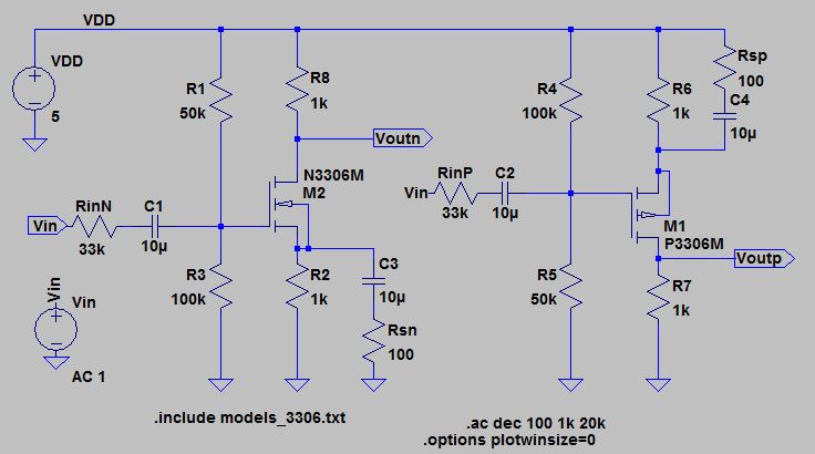
We know that the 50k resistor and the 100k resistor is in parallel, therefore the input resistance would be 33k.
In order to measure this value, we added our own 33k resistor in series to this input resistance.
This would effectly divide our input voltage by half, giving us half our output voltage.
Knowing that this gives us half out output voltage we can then conclude that the input resistance is very close to our calculated input resistance.
| NMOS | PMOS |
 |  |
Simulation to show what's to be expected by placing resistor with the input resistance.
Output resistance:
We know that our output resistance is 1k in parallel with 1/gm.
In order to measure this value, we add a resistor with the same value (55 for NMOS and 94 for PMOS) in series with a large capacitor and connect it parallel to the 1k resistor.
We use a large capacitor in this case so that we can avoid messing up the biasing.
Knowing that this gives us half out output voltage we can then conclude that the output resistance is very close to our calculated output resistance.
| NMOS | PMOS |
 |  |
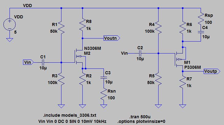
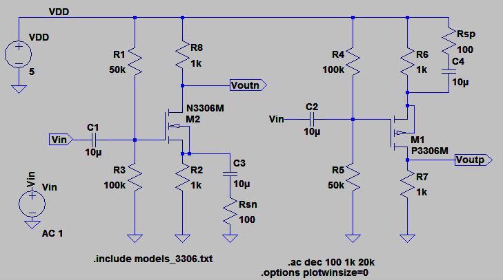
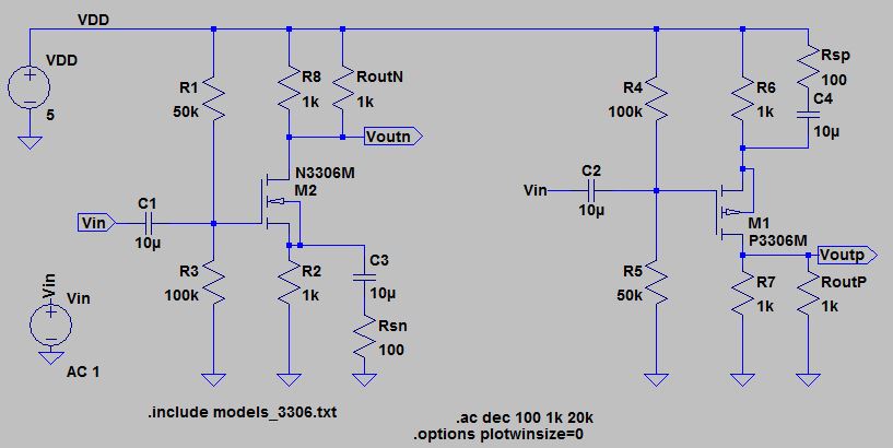
Below is the schematic for the common-source amplifier.
The common-source amplifier is similiar to the common-drain, the input is coming into the gate of the mosfet however the output is going out the drain compared to the source of the common-drain amplifier.
Thus making the common node the source terminal of the mosfet.
DC simulation:
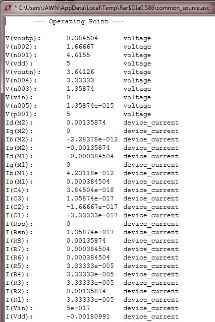
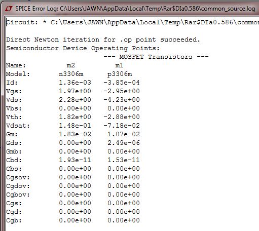
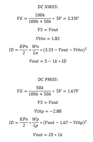
DC hand calculations:
AC simulation:
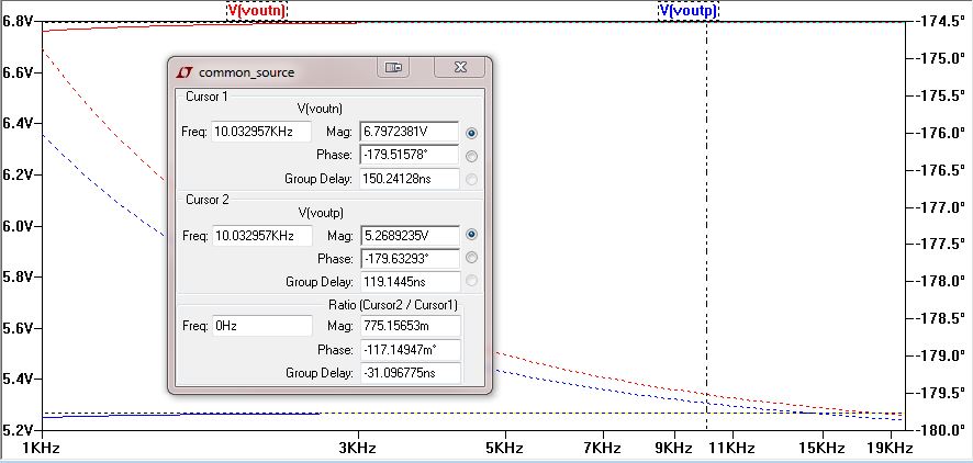
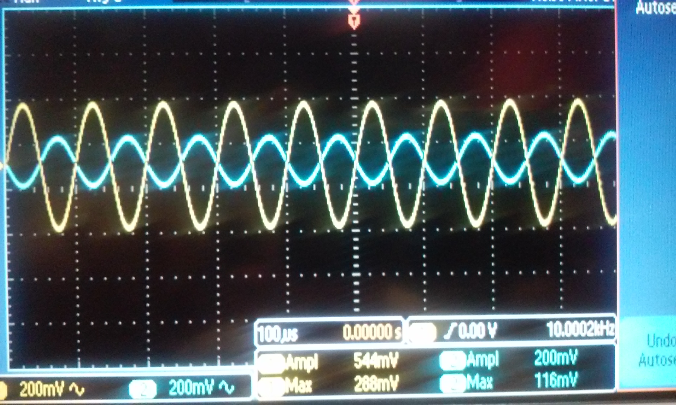
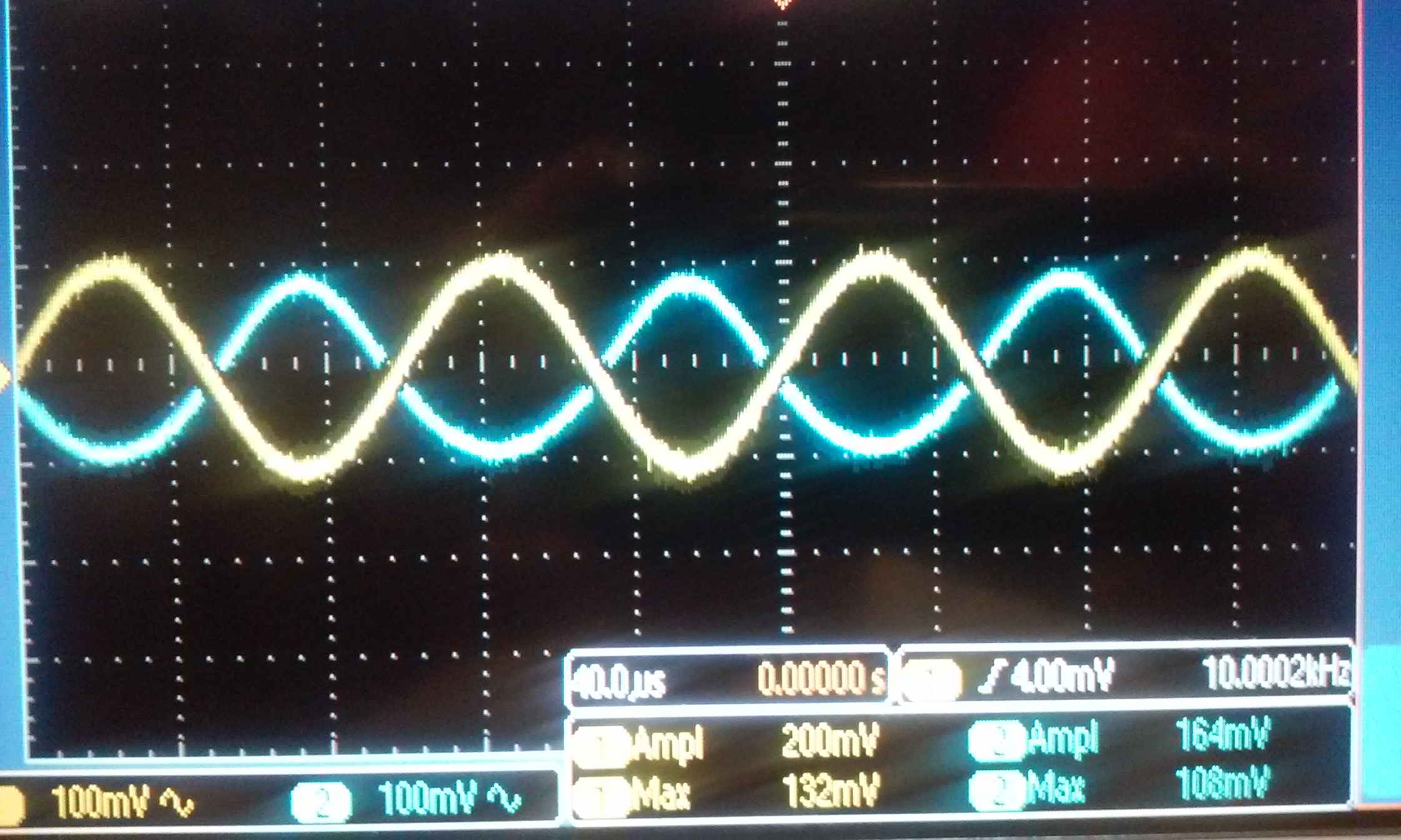
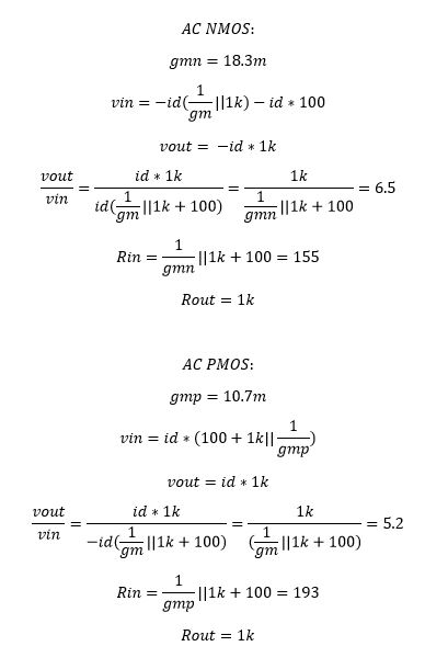
Since Vin is 10mV, we can see that the NMOS has a gain of -7 while the PMOS has a gain of -5.
You can see that the gain is negative since the graph is out of phase.
AC hand calculations:
The source resistance, Rsn or Rsp, will cause the gain to decrease if the source resistance is increased.
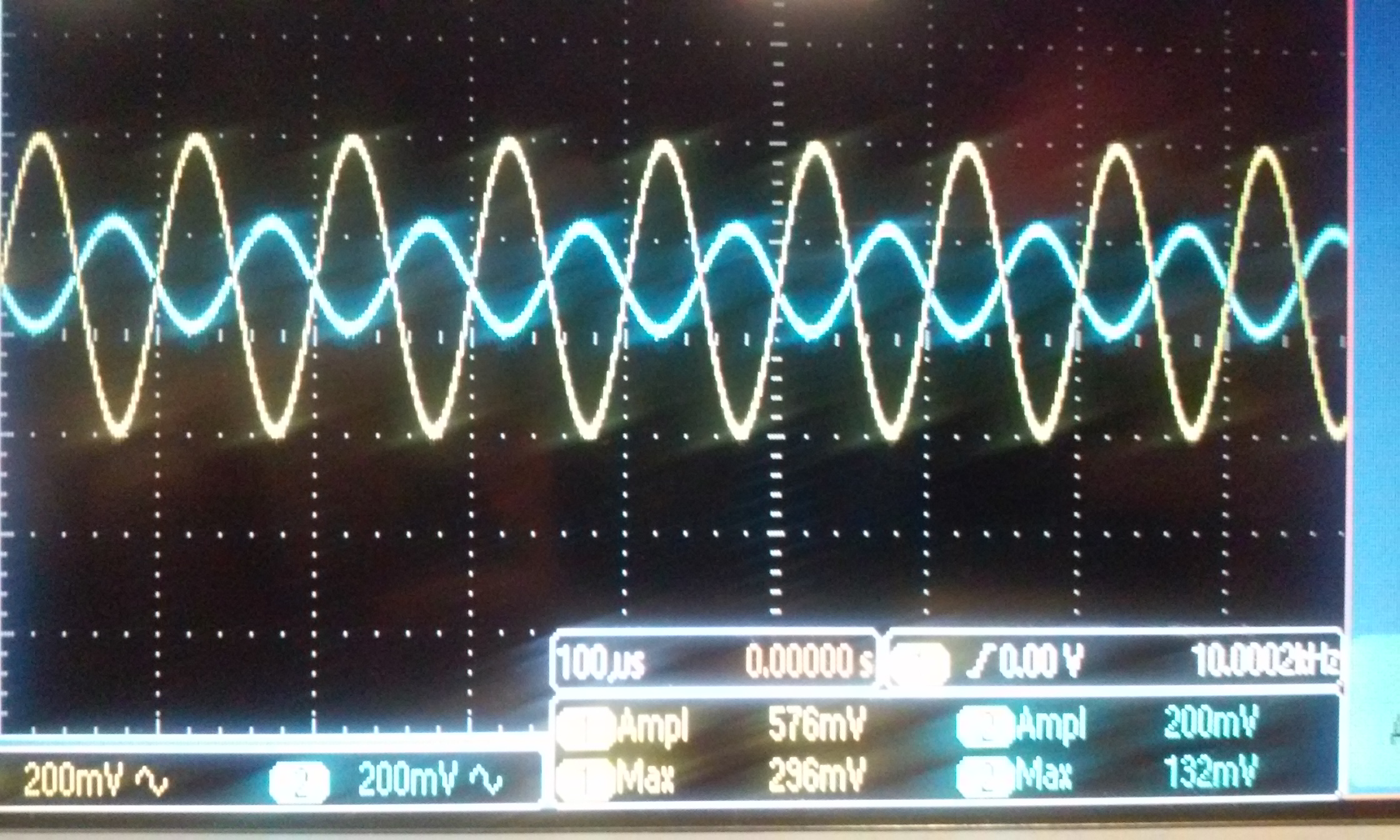
Experiment:
| NMOS | PMOS |
 |  |
| NMOS | PMOS |
 |  |
| NMOS | PMOS |
 |  |
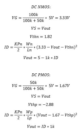
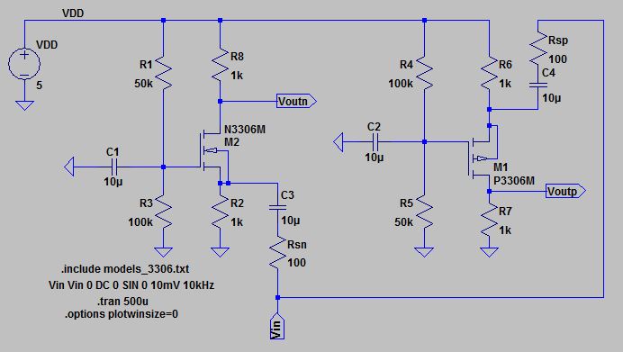
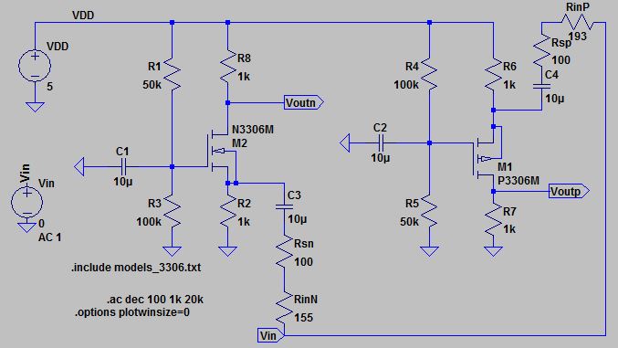
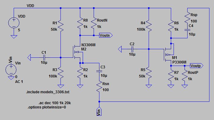
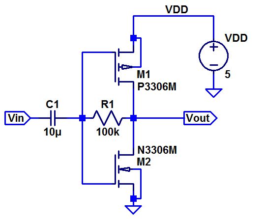
Below is the schematic for the common-gate amplifier.
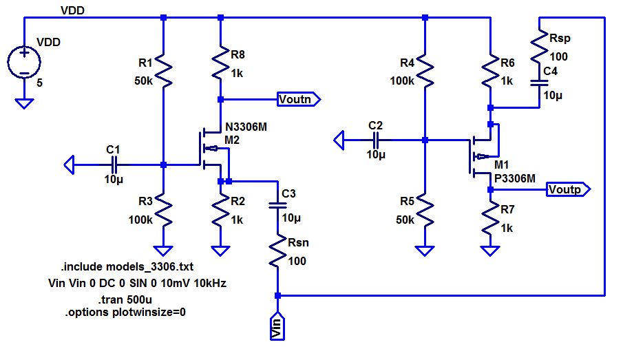
The common-gate amplifier just like the other two has it's input at the source terminal and it's output at the drain terminal, leaving the gate to be the common node.
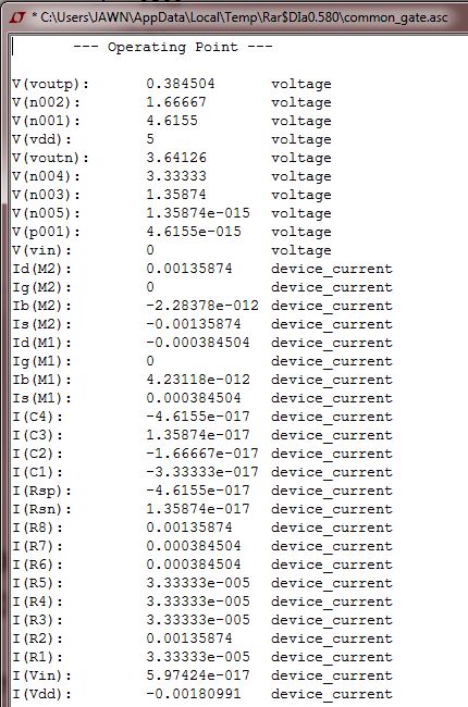
DC simulation:
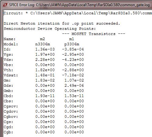
DC hand calculations:
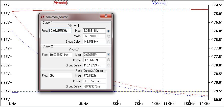
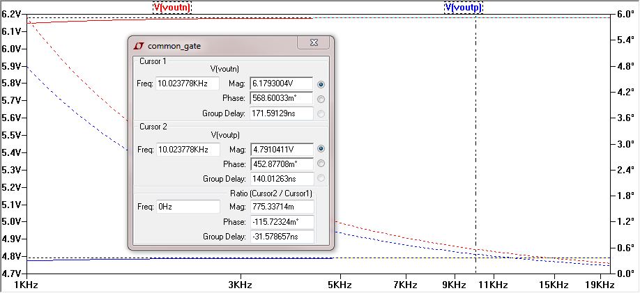
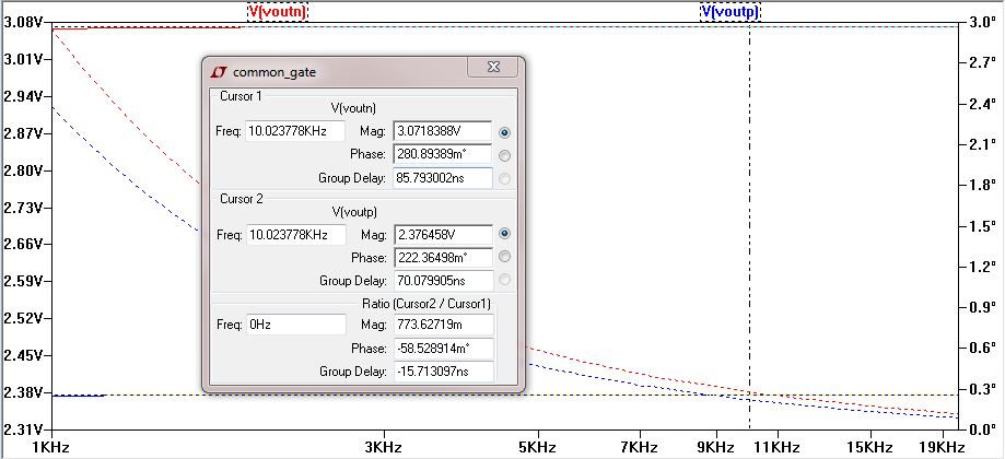
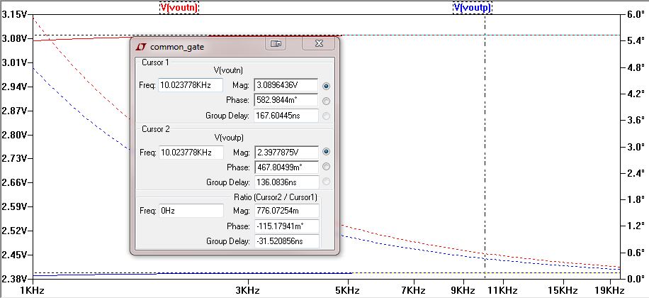
AC simulation:
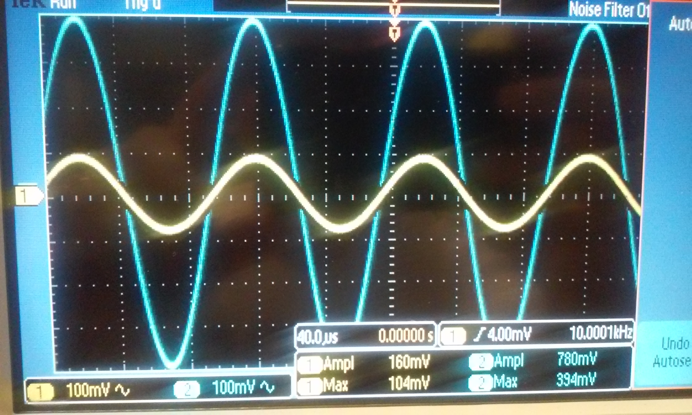
Since Vin is 10mV, we can see that the NMOS has a gain of -7 while the PMOS has a gain of -5.
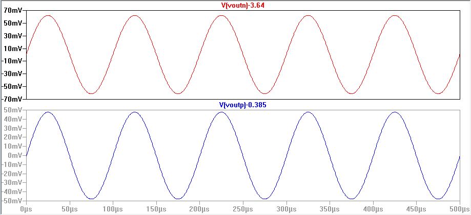
AC hand calculations:
The source resistance, Rsn or Rsp, will cause the gain to decrease if the source resistance is increased.
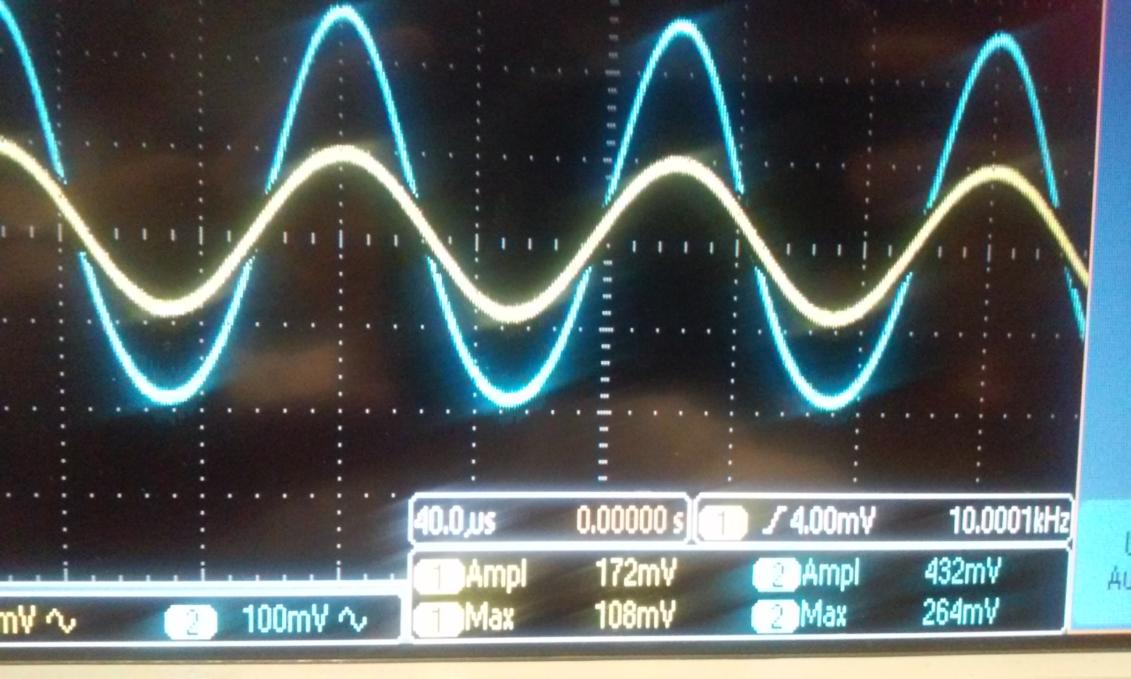
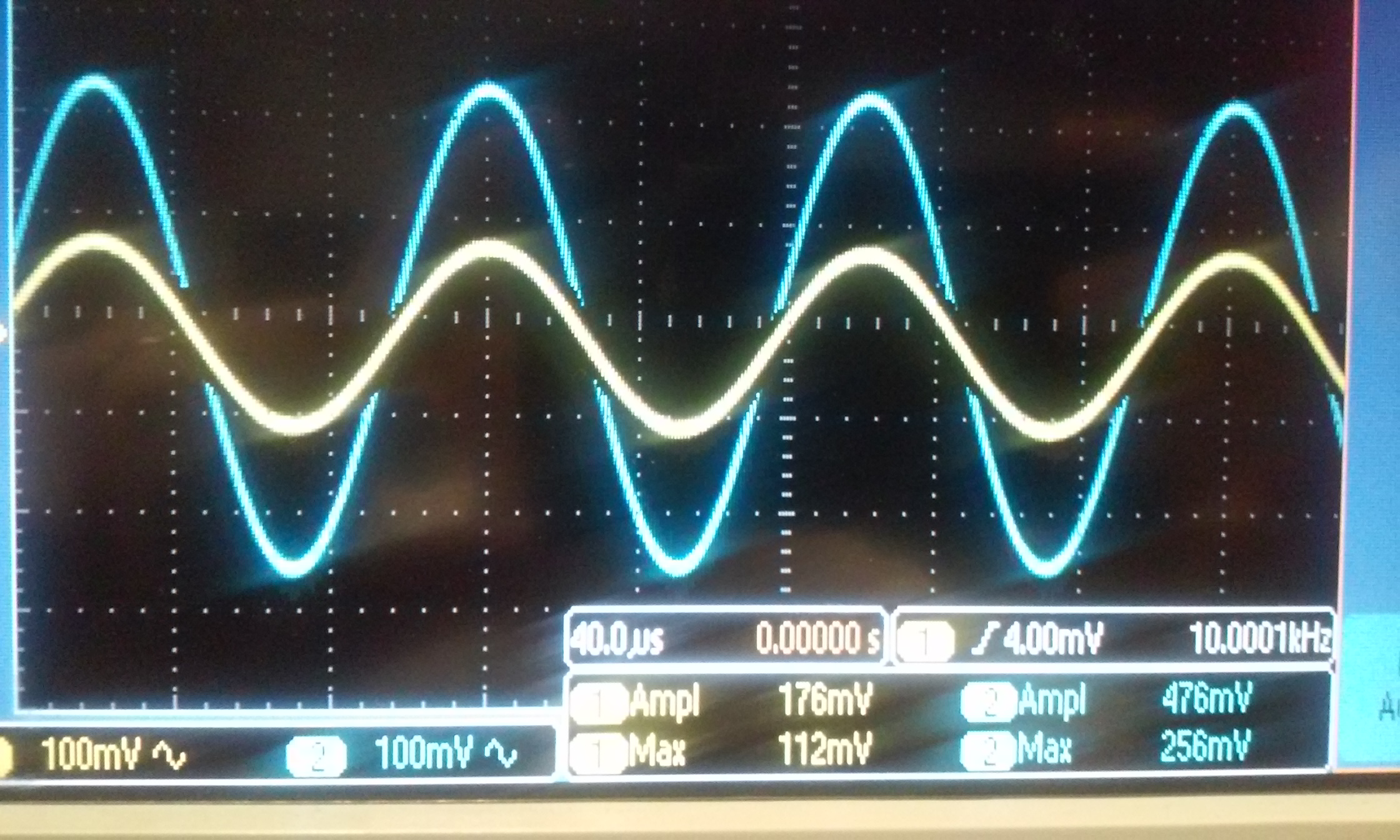
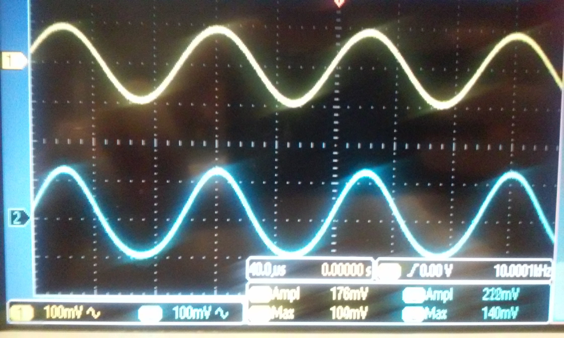
Experiment:
| NMOS | PMOS |
 |  |
| NMOS | PMOS |
 | 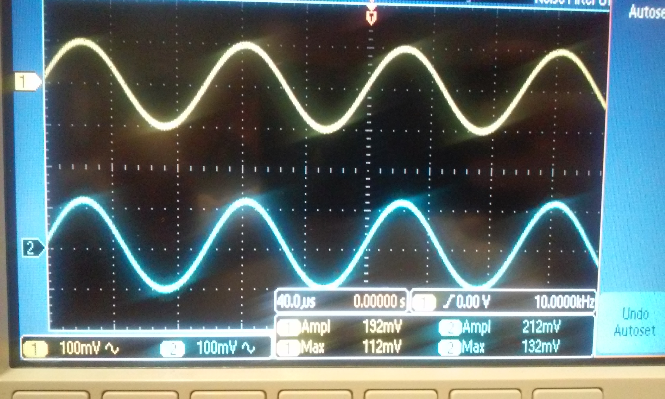 |
| NMOS | PMOS |
 |  |
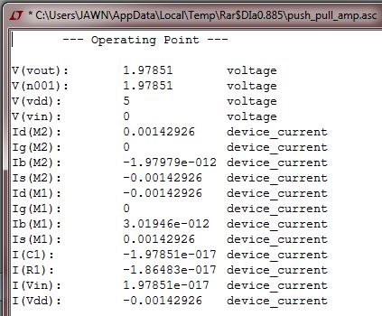
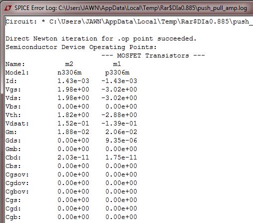
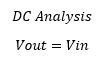
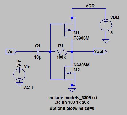
DC simulation:
DC hand calculations:
AC hand calculations:
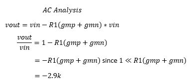
We can see that the gain is directly influenced by the resistance value of R1.
Therefore if we increase the value of resistor our gain would also increase.
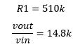
Theoretically our gain would be 5 times as much compared to the 100k resistor if we use a 510k resistor.
AC simulation:
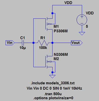
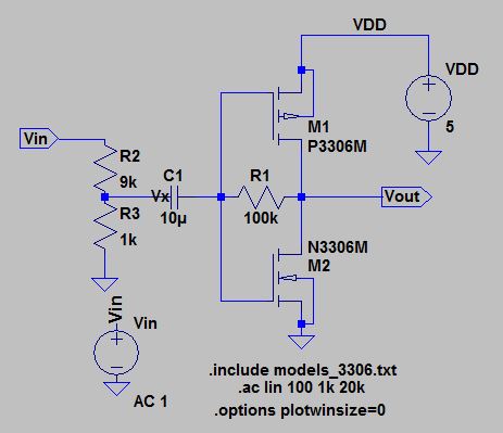
R1 = 100k
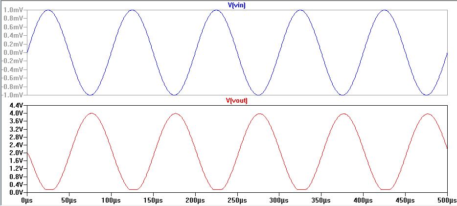
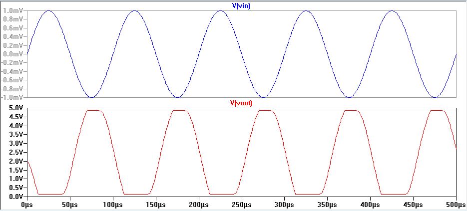
We can see that our gain with the 510k resistor starts to saturate and go towards VDD and GND.
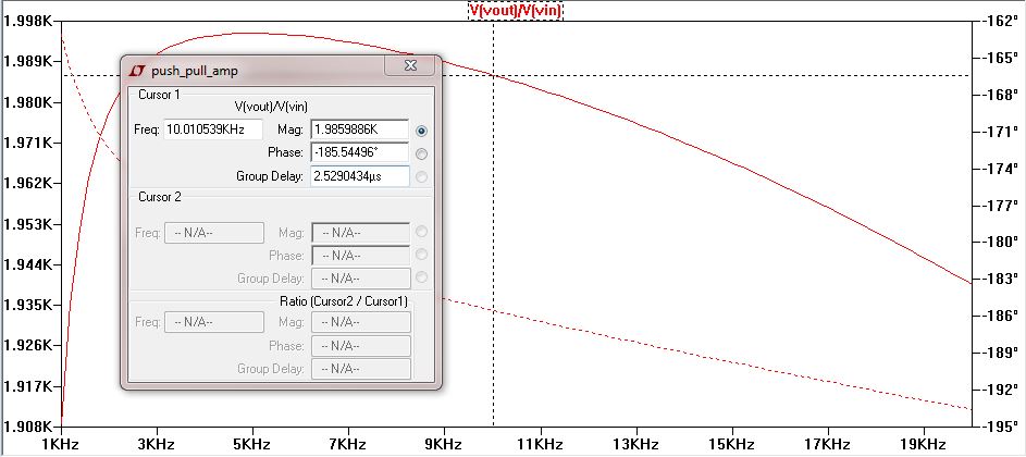
Using an AC analysis we might be able to get an actual gain value.
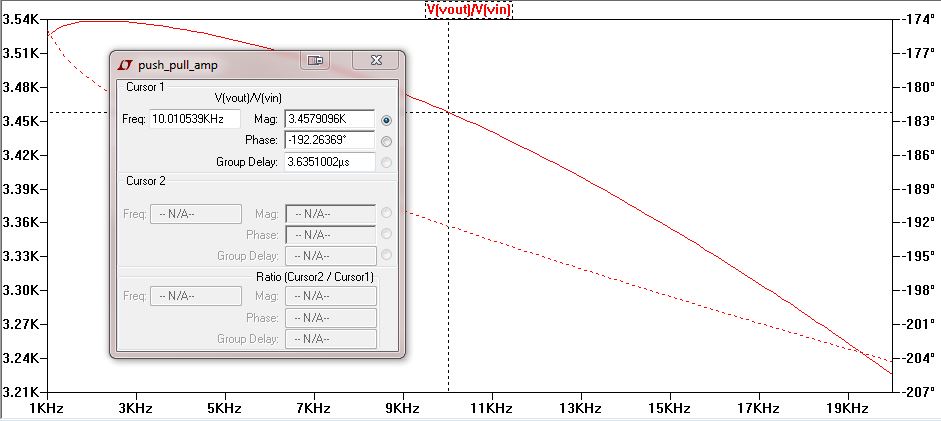
We calculated a gain of -2.9k however our sim only showa gain of -1.99k.
Trying this using the 510k resistor, we should still get 5 times what we got with the 100k resistor, however this is not the case.
The saturation that happens as the gain gets too large causes the output gain to not be represented acrruately.
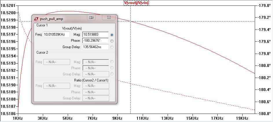
In order to fix this problem we use a voltage divider at the input in order to see the large gain.
Here we are simply just use a simple voltage divider made with a 1k and 9k resistor, making the voltage of vin 0.1 times smaller.
Here we can see the gain is 10 with the 100k resistor.
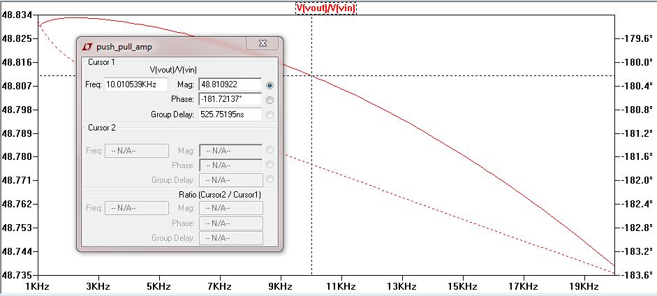
Here we can see the gain is 48 with the 510k resistor which is much more close to a increase of 5 times the gain when comparing the 100k resistor gain.
Experiment:
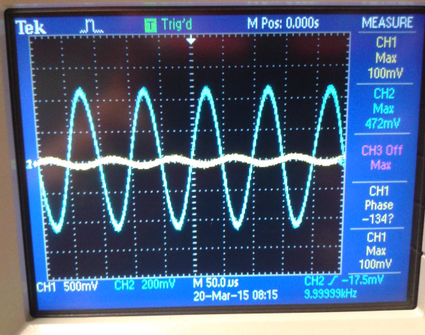
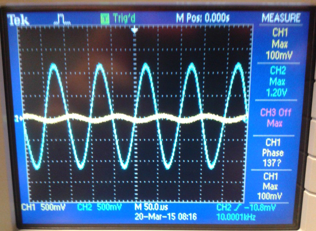
Our experiment was done starting with the voltage divider, even though it says channel 1 is 100mV, it is actually only 10mV
We can see that the gain with the 100k resistor is about 50, but with the 510k resistor is 120.
Even our experiment did not come out as expected with the gain, but we can say that as we increase the resistor value of R1, our gain will also go up.
| R1 = 100k | R1 = 510k |
 |  |
From this lab, we learned the three different single stage amplifiers, common-source, common-drain, common-gate. We learned how to identify one from the other and how to determine the gain of each amplifier.
We learned how to measure the input and output resistance through adding a resistor and determining how the gain is affected.
We also learned how the push-pull amplifier works and how you can change the resistor in order to increase or decrease the gain, however it's uses start to fall off when approaching very high gains or high voltages.
Back up:
Make sure you back up your whole CMOSedu folder with all your labs by compressing the folder and sending it to yourself through email.