ECE 421L - Lab 3
John Huang
Huangj19@unlv.nevada.edu
Spring 2015
Lab description:
Lab 3 is to learn the basic op-amp functions using the LM324 op-amp.
We will learn basic terms associated with majority of the op-amps.
In the lab we will ultilize the LM324 op-amp.
Here is the datasheet associated with the op-amp LM324.
We will be using the following values for the experiment: VCC+ = +5V and VCC- = 0V.
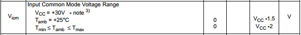
1.
Knowing that the inverting input, Vp, is at the same potential as the
inverting input, Vm, (called the common-mode voltage, VCM) what are the
maximum and minimum allowable common-mode voltages?
According
to the datasheet, the maximum allowable VCM is VCC+ = -1.5V and VCC- =
0V at +25 degrees Celcius (ambient temperature).
This
means that the range of our op-amp operation would be between 0 to
3.5V. If VCM was to be out of this range then the op-amp would not
operate.
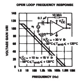
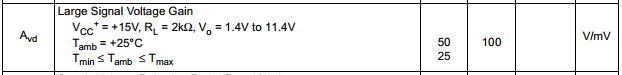
2. What is a good estimate for the op-amp's open-loop gain?
According to the datasheet's graph of the open loop frequency response, we can estimate that the open-loop gain would be 100dB.
We can see that the electrical characteristic table that large signal voltage gain is 100.
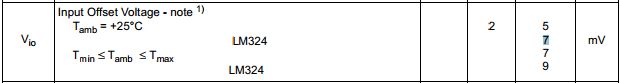
3. What is a good estimate for the offset voltage?
According
to the datasheet, the offset voltage is around 7mV at ambient
temperatures. For worst case design we would use the maximum offset
voltage, which is 9mV.
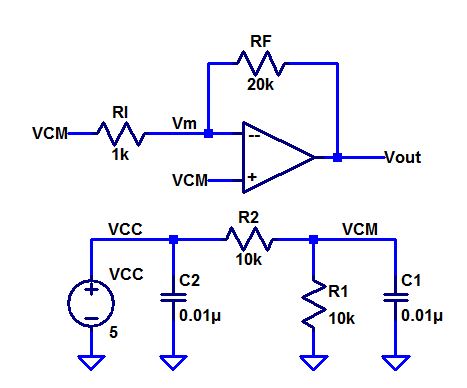
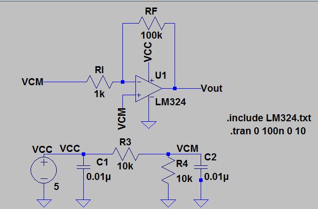
Now we construct the following circuit seen below.
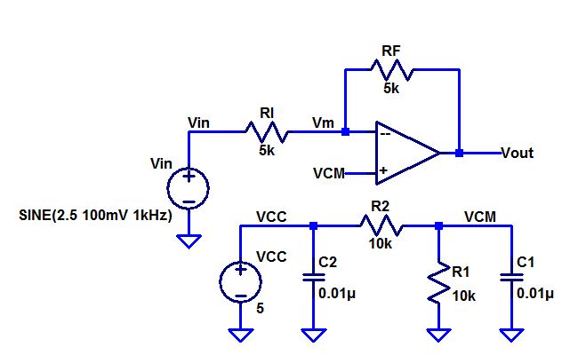
4.
Idealy our VCM would be half of the VCC, input voltage (5V), which
would be 2.5V. VCM should not change unless we change VCC. We can see
that VCM is a result from the voltage divider from VCC.
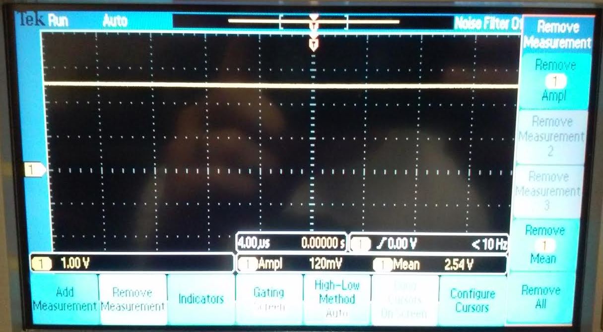
During our experiment we measured a VCM of 2.54V which is close to the theoretical voltage.
5.
The ideal closed-loop gain for our circuit based on an inverting
typology since our input is at the negative terminal of the op-amp.
|Vout/Vin| = -RF/RI = -5k/5k = -1
6. The output swing from our experiment goes from 2.38V to 2.66V. This output swing is centered around our VCM voltage 2.54V.
This is due to the input and output being roughly 2.5V and having an offset voltage set at 100mV from the AC source.
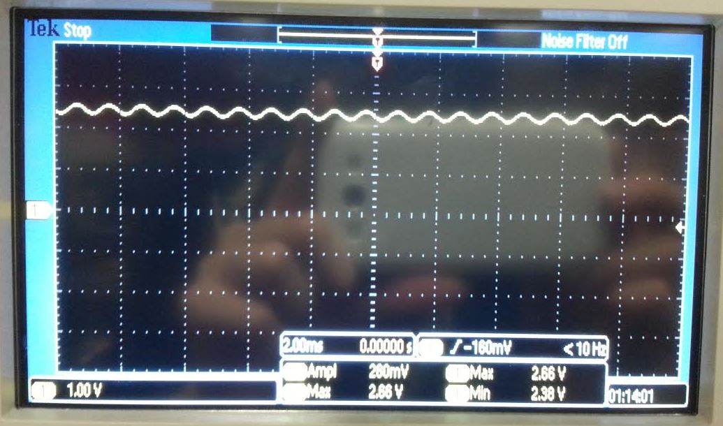
If the voltage of the input is larger than VCM then the output swing would not be centered around VCM and instead go down.
We know that the gain of our idea close loop gain is |Vout/Vin| so as the input voltage increases the output will go down.
7. The maximum allowable input signal amplitude would be our VCMmax - Vin = 3.5 - 2.5V = 1V.
This is limited because of our VCC+ being 5V causing out VCMmax to be 3.5V.
If
we increase this amplitude too much it will force the mosfet to go into
triode, which wopuld affect the open loop gain and output voltage.
8.
If the magnitude of the gain is increased to 10, then the maximum
allowed input signal would only be 1/10th of its original input.
We know that Vout = AOL*(Vp-Vm), if AOL = 10 then we would end up with Vout = 10*(Vp-Vm) => Vout/10 = Vp-Vm.
9. The capacitors that are connected from VCC and VCM to ground is decoupling capacitors.
The
values of the capacitor are not critical because they only help
stablize the voltage being driven by filtering out the noise.
Increasing the values of the capacitor does not affect the voltages of VCM or VCC because they are DC voltages.
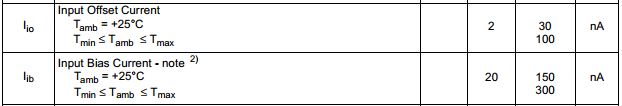
10. The op-amp has a input bias current that flows out of the op-amps input of typically 20nA.
The input offset current is given by the datasheet. We can see that it is between 30-100nA depending on the temperature.
It
is noted that the direction of the input current is out of the IC. This
current is essentially constant, independent of the state of the output
so no loading change exist on the input lines.
The
input offset current is the difference between the current going
through the positive (Vp) and negative (Vm) terminals of the op-amp.
If we increase the resistances of RF and RI we will only decrease the current even more considering it is already in nA.
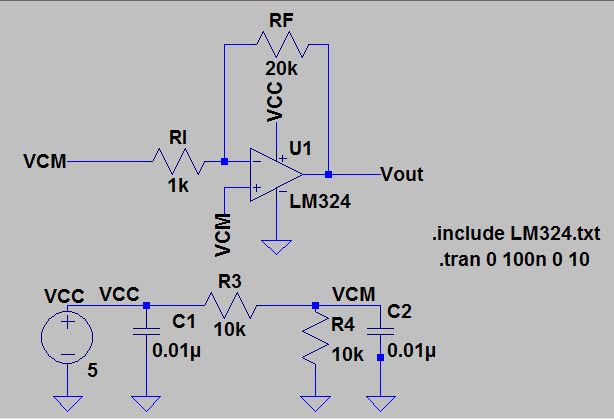
The following circuit is used to answer the following questions.
Since there is no AC signal going through the op-amp we can measure the op-amp's offset a different way.
We
can see that Vm and Vp's input is VCM, however since the op-amp is deal
with no offset, we can assume that there is no current flowing through
RF and RI.
This would mean that Vout should be equal to Vm and VCM. The difference between Vout and VCM is the offset voltage.
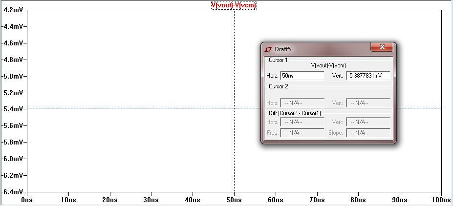
The LM324 text file I used can be found here.
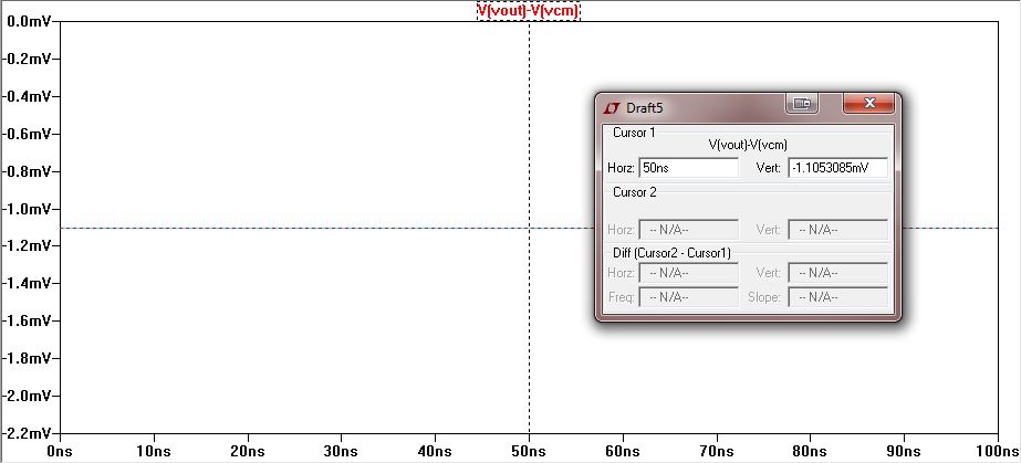
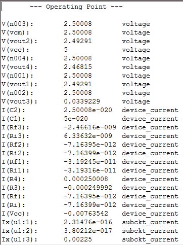
Offset voltage of 1.105mV
With a gain of 100.
Offset voltage of 5.38mV
Here are the offset voltage of 4 different op-amps:
| Op-amp | LT1002 | LT1001 | LT1006 | LT1007 |
Gain 20
Offset (mV) | 0 | 0 | 0.170 | 0 |
Gain 1000
Offset (mV) | 592 | 7 | OFF | 32 |
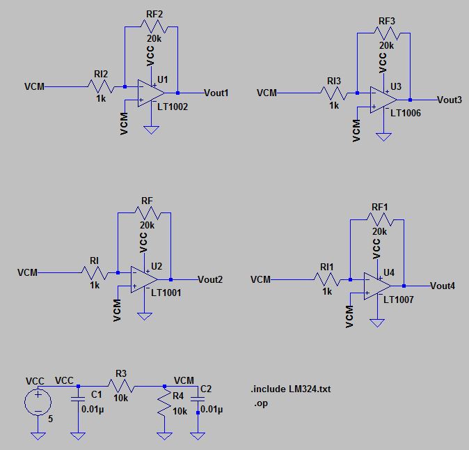
Gain: 20
Offset = Vout - VCM for each op-amp.
Gain 1000
Offset = Vout - VCM for each op-amp.
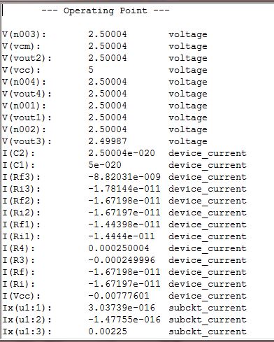
At a gain of 20, you can see that from running an operating point on
the op-amps, you can not really measure the really small offset
voltages that they might have compared to if you measured each one
seperately.
It can be said that each offset voltage of the op-amp is
insignificantlly small even for the LT1006 which had a offset voltage
of 170uV.
In order to get more data, I boosted the gain to 1000, in
order to see a signifcant change in offset. Note that the VCM also goes
up as the gain increases.
Here the op-amp of LT1006 actually turns off.
Back up:
Make
sure you back up your whole CMOSedu folder with all your labs by
compressing the folder and sending it to yourself through email.

Return to my lab reports
Return to student lab reports
Return to ee420L webpage