ECE 421L - Lab 2
John Huang
Huangj19@unlv.nevada.edu
Spring 2015
Lab description:
Lab 2 is used to explain the function of a compensated probe.
We will see the differences between an undercompensated, overcompensated and compensated probe.
We will understand how the 10:1 compensated probe is made, based off schematics.
We will see the differences between measuring data using a compensated probe compared to a regular set of wires.
1. Scope waveforms of a 10:1 probe.
| Undercompensated | Overcompensated | Compensated |
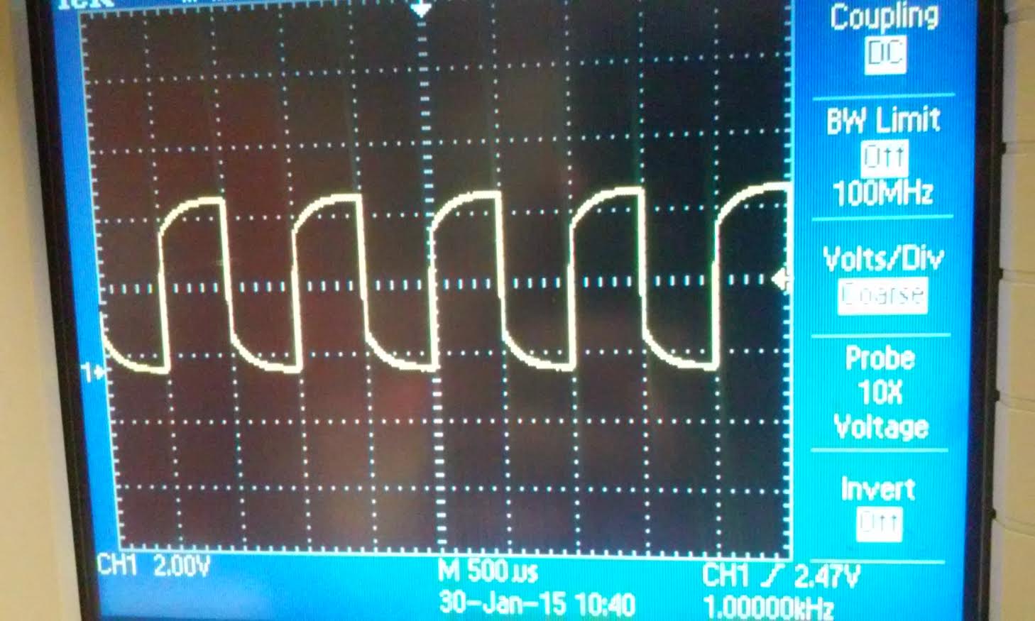 | 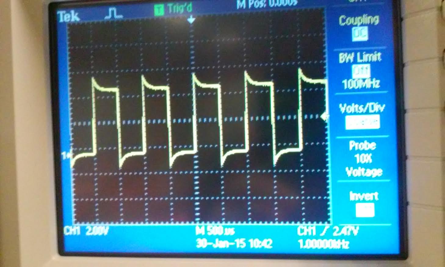 |  |
2. Our probe was set at 10:1, the probe we used did not have an option to switch from 1X or 10X.
The oscilloscope automatically detected that the scope was a 10x scope.
3. Below is the schematic of a 10:1 probe scope.
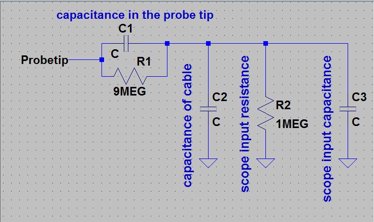
4.
Here we assume that the scope input capacitance is 18pF and
the cable capacitance is 90pF in order to show that the input
voltage of the scope is 0.1 volts to the probe tip.
We must find the Vout of the schematic.
We set C1 = 1/9(C2+C3) = 1/9(108) = 12pF
Now we have to solve for the impedance of Z1 (C1 and R1) and Z2 (C2, C3 and R2).
Z1 = C1 || R1
= 9MEG || 1/jw12p
= (9MEG/jw12p)/(9MEG+1/jw12p)
= 9MEG/(1+jw*9MEG*12p)
Z2 = R2 || (C2+C3)
= 1MEG || 1/jw180p
= (1MEG/jw108p|/(1MEG + jw108p)
= 1MEG/(1+jw*1MEG*108p)
Vout = Z2/(Z1+Z2)*Vin
= [1MEG/(1+jw*1MEG*108p)]/[1MEG/(1+jw*1MEG*108p) + 9MEG/(1+jw*9MEG*12p)]
= 1MEG/(9MEG + 1MEG)*Vin
= 1/10 Vin
This shows that the scope input voltage is 1/10 the probe input voltage.
5.
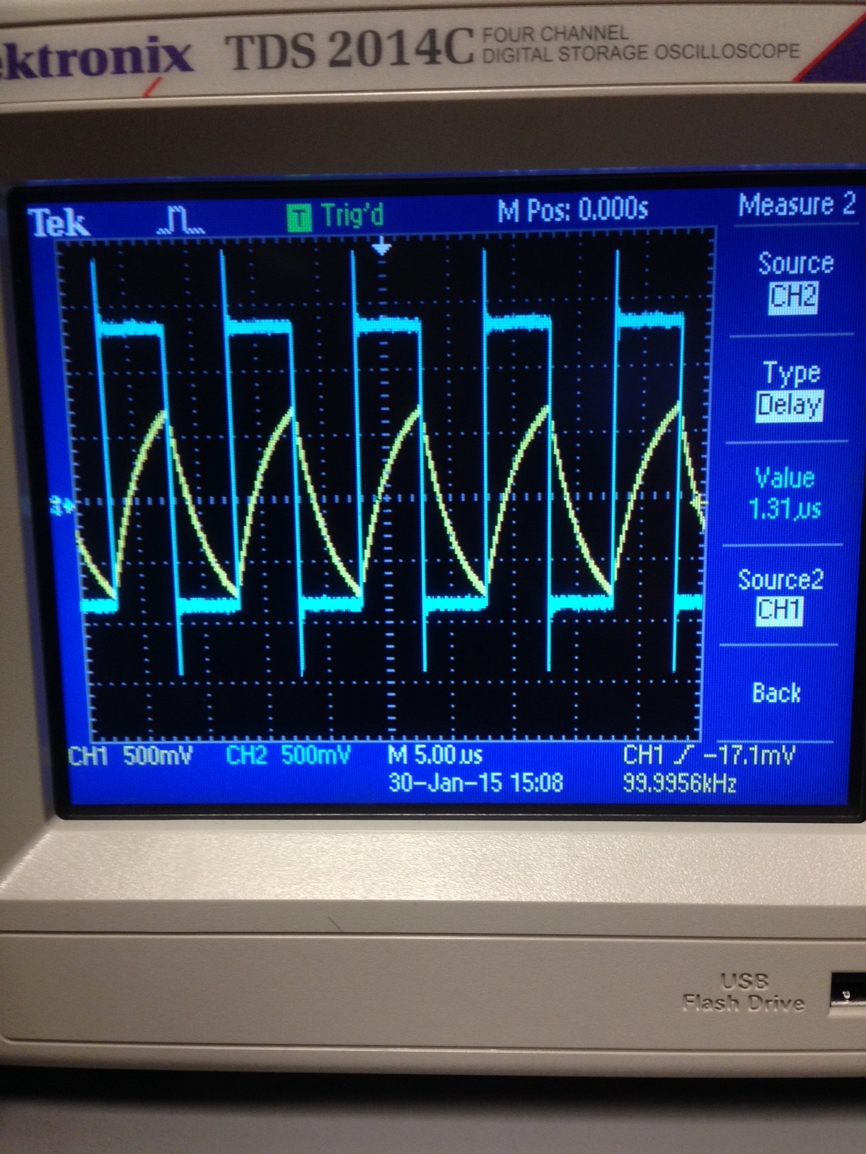
In order to measure the capacitance in the scope, we devised an
experiment using a simple RC circuit using a pulse as an input voltage.
The
point of this RC circuit is the measure the time delay caused by the RC
circuit, which allows us to use the time delay formula td=0.7*R*C in
order to calculate the capacitance.
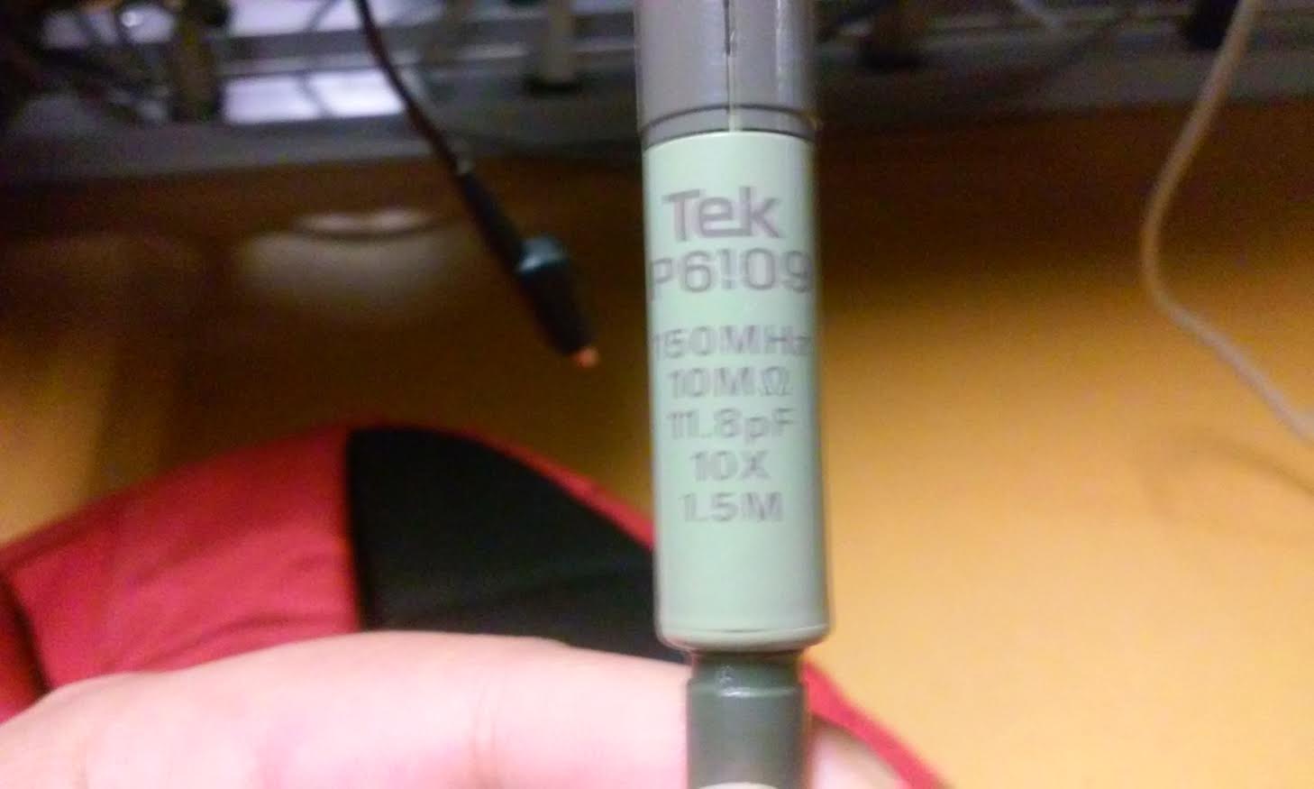
We used a resistor with a value of 100k and the scope probe as our capacitor.
We then used another scope probe to measure the time delay.
We got a time delay of 1.31 us.
C = td/(0.7*R)
= 1.31u/(0.7*100k)
= 18.71pF
Now that we have the experimental value, we used a capacitor meter to measure the capacitance across the scope probe.
The capacitor meter gave us 50pF as the capacitance.
Here is the oscilloscope showing the time delay of 1.31us.
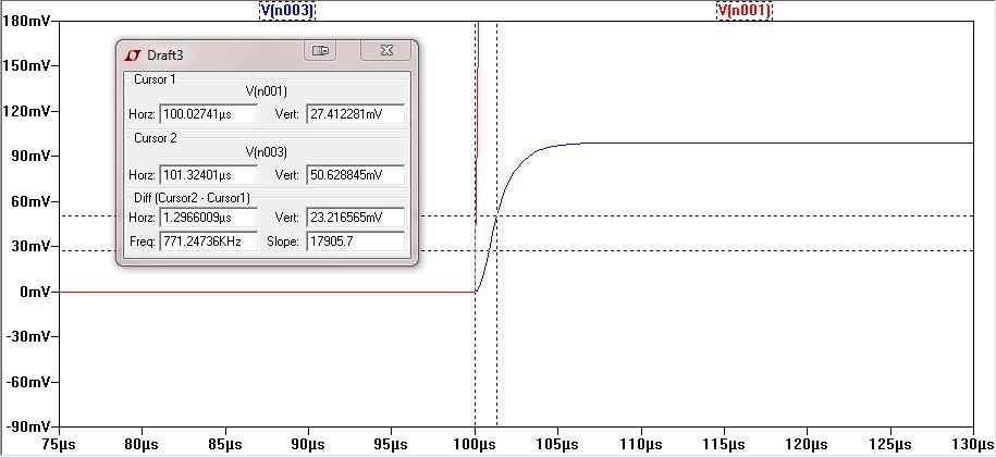
Using ltspice we can verify the time delay by setting the input capacitance as 18pF that we calculated.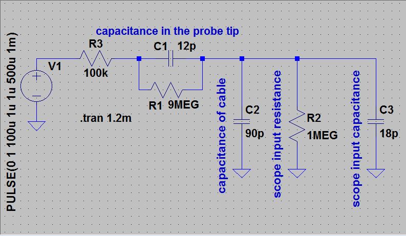
We can see that at 50mV the delay was 1.30us which is pretty much spot on to our experimental reading.
Even
though the capacitor meter and our measured capacitance was off by
150%, it is still within the ball park considering how small a pF is in
terms of measurement.
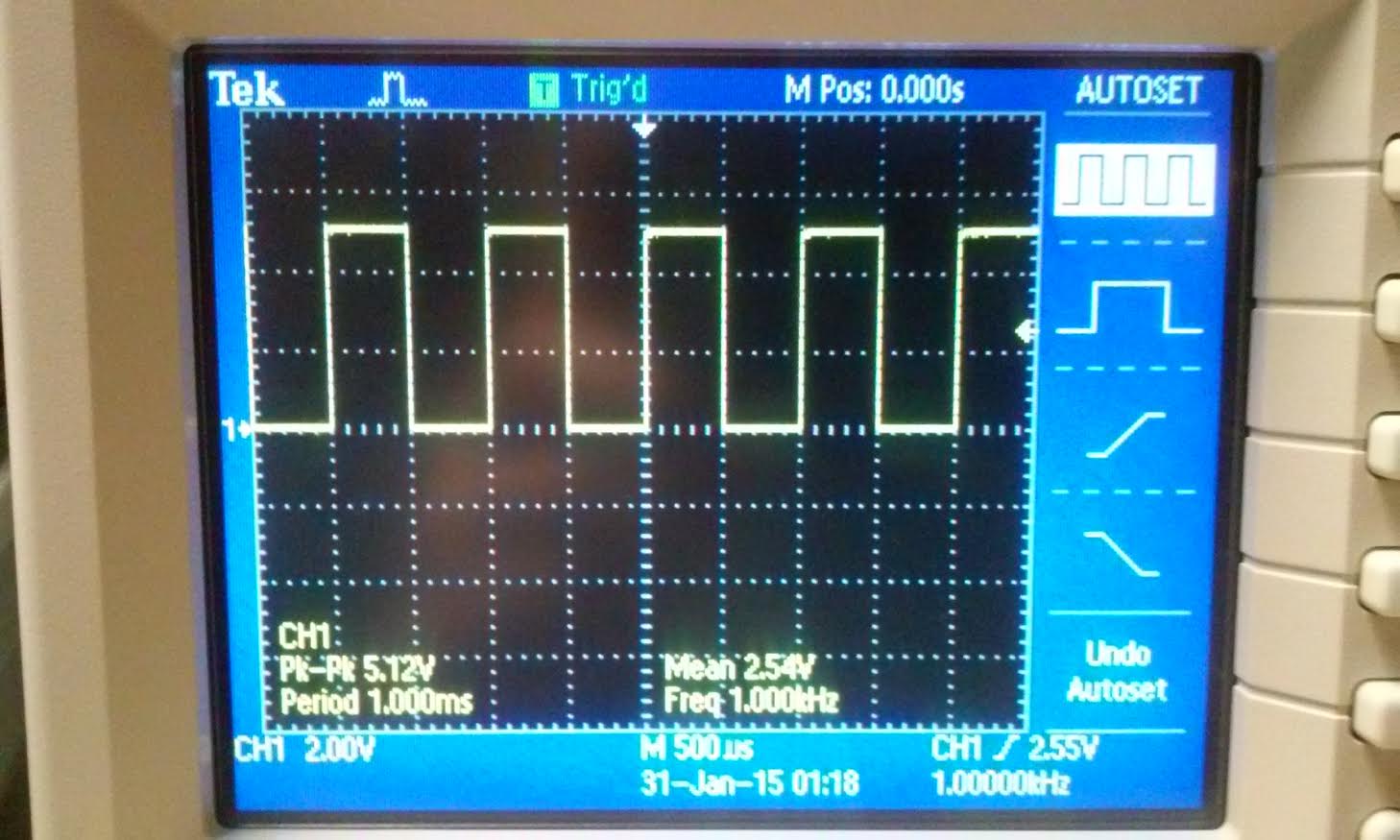
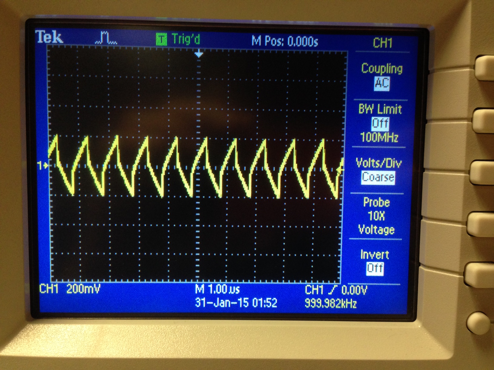
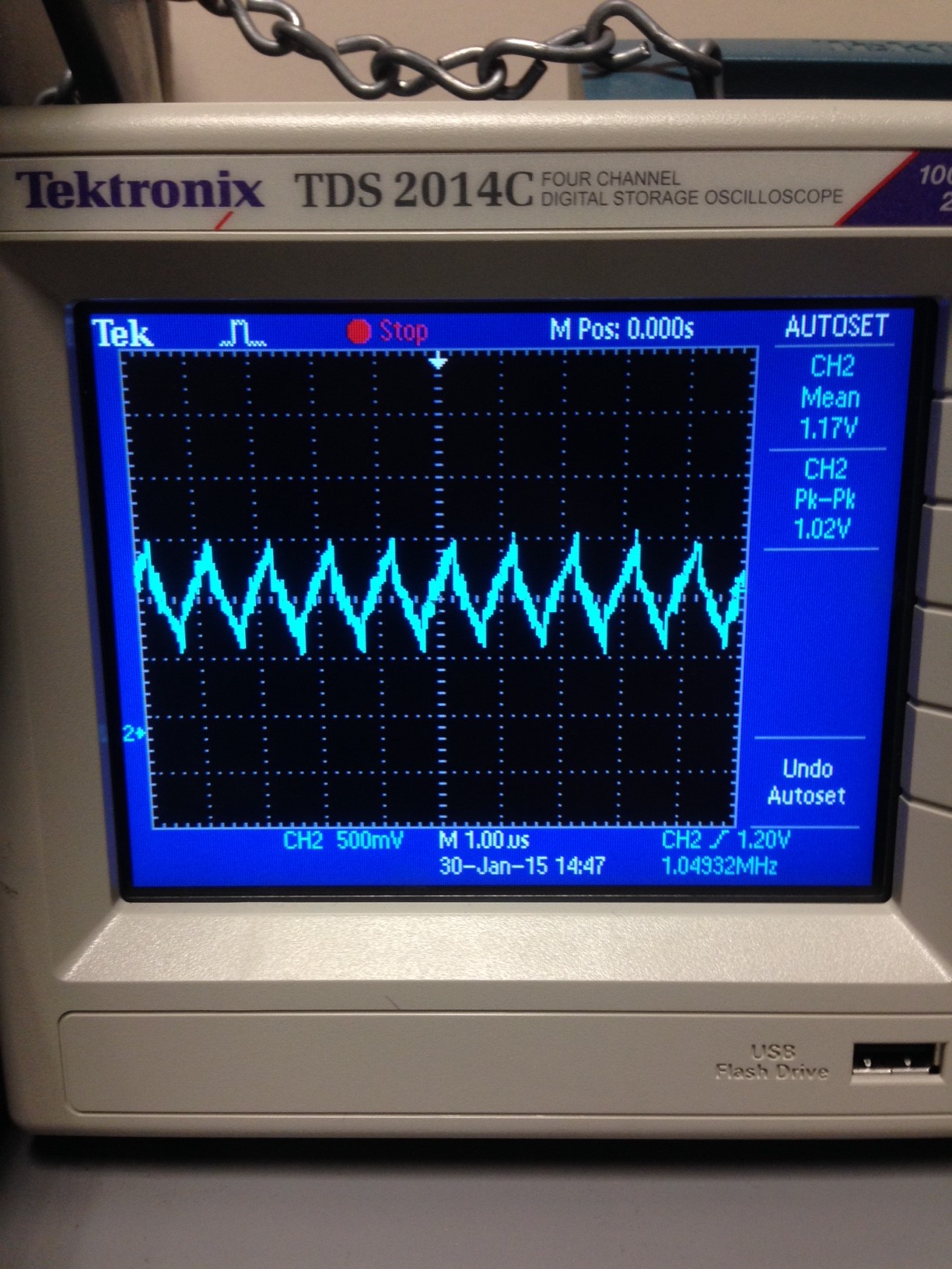
6. We built a voltage divider using two 100k resistors and measured the outputs using a compensated probe and a straight cable.
In the two pictures we can see that the compensated probe helps show a much more stable and accurate reading.
We
can see that the peak to peak voltage on the compensated probe is about
400mV which is close to the theoretical value of 500mV.
While
the straight cable we are getting a peak to peak voltage of 1.02 V
which is caused by the signal charging and discharging too quickly.
We
can also factor in that the straight cable has resistance that is not
usually accounted for compared to the compensated probe.
| compensated probe | straight cable |
|  |
7.
Q:
Briefly discuss how you would implement a test point of a printed
circuit board so that a known length of cable could be connected
directly to the board and not load the circuitry on the board.
A:
A good way to implement a test point on a printed circuit board would
be adding a resistor and a capacitor in parallel before connecting the
cables, this you can say would be just like using a compensated scope
probe.Conclusion:
We
can see the use of the compensated probe in order to measure accurate
points of data. We can also implement our own scope probe when
measuring directly on a PCB if needed to be in order to prevent loading
the circuitry on the board.
Back up:
Make
sure you back up your whole CMOSedu folder with all your labs by
compressing the folder and sending it to yourself through email.
Return to my lab reports
Return to student lab reports
Return to ee420L webpage