2VDSsat+VSG
or Vref+VGS+VSG
its pretty safe to say Vref+VGS+VSG is the larger which works out to be
1.2+0.8+0.8=2.8V

Id=0.9mA
R=58Ohms
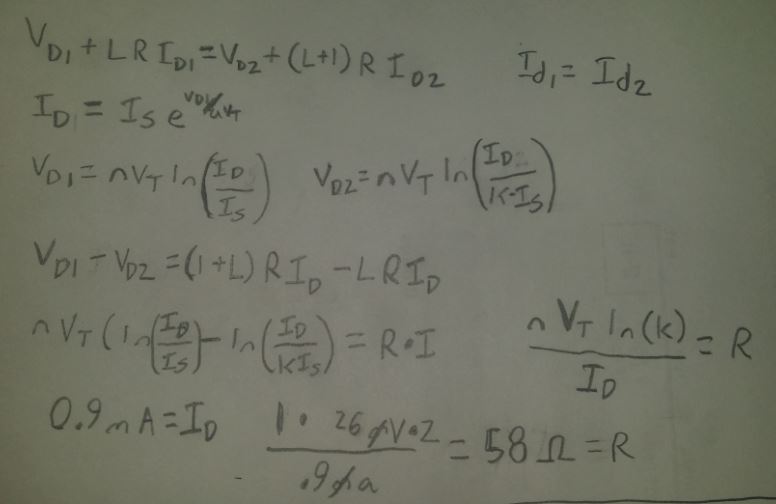
L=8.41
R1=550Ohms
R2=500Ohms

Lab Final Project - ECE 420L
Project - using as many diodes, resistors, and capacitors as needed, along with two CD4007 chips from the same production lot (see date code on the top of chip) to ensure current mirrors are possible, design and build a bandgap voltage reference (BGR). Your report, in html, should detail your design considerations, simulation results (using the models you generated in lab 8), and measured results showing the BGR's performance (how the reference voltage changes with VDD). It would be good, but it's not required, if you could also characterize the BGR performance with temperature. Your report is due at the end of lab on Friday, May 8. Access to your CMOSedu.com accounts will be removed at this time.
For our Bandgap reference we chose to use the differential amplifier BGR topology, with PMOS devices used to isolate the diff amp. seen in figure on page. This design creates a very consistent bandgap even for lower values of VDD and maintains its reliability with temperature changes. one thing to remember about this design is that since it uses PMOS to isolate the diff amp the inverting and non inverting inputs need to be switched when compared to a Diff-amp BGR without pmos isolation. Its minimum VDD will be about 2.5V as you can see below in the hand calculations.
the models we used in this design can be found here: MOS.txt
| Here is a rough schematic for the Band Gap it is useful for finding the minimum VDD which is the greater of 2VDSsat+VSG or Vref+VGS+VSG its pretty safe to say Vref+VGS+VSG is the larger which works out to be 1.2+0.8+0.8=2.8V | |
| Finding the Value for R Id=0.9mA R=58Ohms |
|
| Finding th Value for L L=8.41 R1=550Ohms R2=500Ohms |
|
| Schematic | Simulation Results |
 |
|
| this is the same topology as above but with a 15meg "start up" resistor which forces the voltage at node 3 to increase to its required value, to get VGm1 to its threashold voltage. |
|
| here you can see the pin out for the CD4007 chip |
 |
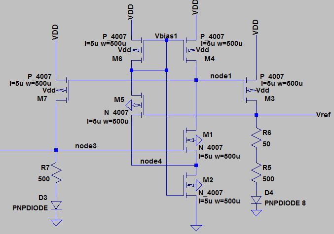
| Our component level schematic for this topology can be seen in the following picture: |
|
another advantage of this topology can be demonstated in the above picture. because of how the NMOSes and PMOSes are connected it allows for minimal chip use as two of the biggest factors, when dealing with minimizing the quantity of CD4007 chips, are how the gates at pin 3 6 and 10 connect to both an NMOS and a PMOS and and how the pin 10 NMOS/PMOS are drain connected. With the topology we chose there is 1 set of Gate connected NMOS/PMOS set that means we can use both devices on one gate. This means we need 6 gates which is exactly what 2 chips give us. |
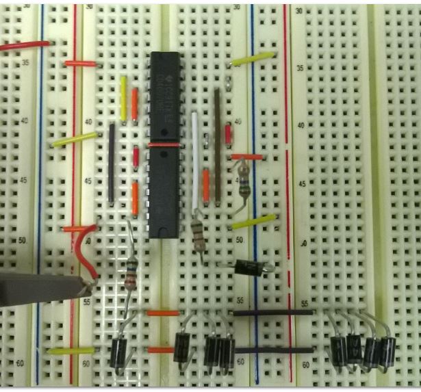
| Here is the physical circuit |
 |
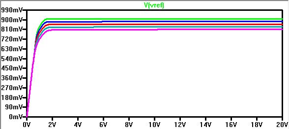
here are the measurements
| Varrying VDD | Varrying Temperature |
| Full Range of VDD on scope | Band Gap at 30 Degrees C |
 |  |
| Turn on Voltage at about 2.8V | Band Gap at 80 Degrees C |
 |  |
| Here you can see the turn on voltage and VREF is about 2.8V like in our hand calcs. however the Vref is higher than the simulations. | for a 50degree C temperature change we only get a -.02V |