Lab 8 - EE 420L
Authored
by Iain Drews drewsi2@unlv.nevada.edu
4/16/2015
Lab
description
In
this lab you will characterize the transistors in the CD4007 and
generate SPICE Level=1 models. Assume that the MOSFETs will be used in
the design of circuits powered by a single +5 V power supply. In other
words, don't characterize the devices at higher than +5 V voltages or
lower than ground potential.
- Experimentally generate, for the NMOS device, plots of:
| ID v. VGS (0 < VGS < 3 V) with VDS = 3 V |  |
ID v. VDS (0 < VDS < 5 V) for VGS varying from 1 to 5 V in 1 V steps, and | ID v. VDS (0 < VDS < 5 V) for VGS = 1V |  |
| ID v. VDS (0 < VDS < 5 V) for VGS = 2V |  |
| ID v. VDS (0 < VDS < 5 V) for VGS = 3V |  |
| ID v. VDS (0 < VDS < 5 V) for VGS = 4V |  |
| ID v. VDS (0 < VDS < 5 V) for VGS = 5V |  |
ID v. VGS (0 < VGS < 5 V) with VDS = 5 V for VSB varying from 0 to 3 V in 1 V steps.
| ID v. VGS (0 < VGS < 5 V) with VDS = 5 V for VSB = 0 |  |
| ID v. VGS (0 < VGS < 5 V) with VDS = 5 V for VSB = 1 |  |
| ID v. VGS (0 < VGS < 5 V) with VDS = 5 V for VSB = 2 |  |
| ID v. VGS (0 < VGS < 5 V) with VDS = 5 V for VSB = 3 |  |
- Experimentally generate, for the PMOS device, plots of:
| ID v. VSG (0 < VGS < 3 V) with VSD = 3 V |  |
ID v. VSD (0 < VDS < 5 V) for VSG varying from 1 to 5 V in 1 V steps, and
| ID v. VSD (0 < VDS < 5 V) for VSG = 1 |  |
| ID v. VSD (0 < VDS < 5 V) for VSG = 2 |  |
| ID v. VSD (0 < VDS < 5 V) for VSG = 3 |  |
| ID v. VSD (0 < VDS < 5 V) for VSG = 4 |  |
| ID v. VSD (0 < VDS < 5 V) for VSG = 5 |  |
ID v. VSG (0 < VGS < 5 V) with VSD = 5 V for VSB varying from 0 to 3 V in 1 V steps.
| ID v. VSG (0 < VGS < 5 V) with VSD = 5 V for VSB=0 |  |
| ID v. VSG (0 < VGS < 5 V) with VSD = 5 V for VSB=1 |  |
| ID v. VSG (0 < VGS < 5 V) with VSD = 5 V for VSB=1.5 (max) |  |
- Assuming
that the length of the NMOS is 5 um and its width is 500
um calculate the oxide thickness if Cox (= C'ox*W*L) = 5 pF.
-
Cox=
5pF
-
C'ox=5pf/(5um*500*um)
2ff/um^2
-
Eox=8.85(aF/um)*3.9=
34.515(af/um)
- TOX=
Eox/C'ox=34.515af/um/ 2ff/um^2 =17.26pm
- From this measured data create a Level = 1 MOSFET model with (only) parameters: VTO, GAMMA, KP, and TOX.
- Nmos
- VTON=1.0
- TOX= 17.26pm
- GAMMA= about .8 (derivded by dividing the threshold voltage by the body-source voltage)
- KP = 2*ID / VDSSAT^2= 2*320uA/1^2= 640u (taken from the 3rd simlation of the second test)
- VTOP=2.0
- TOX= 17.26pm
- GAMMA= about .4 (derivded by dividing the threshold voltage by the body-source voltage)
- KP = 2*ID / VDSSAT^2= 2*200uA=/1^2= 400u (taken from the 3rd simlation of the second test)
- Compare
the experimentally measured data above (the 3 plots) to
LTspice-generated data (again, 3 plots) and adjust your model
accordingly to get better matching.
- Experimentally,
similar to what is seen on the datasheet (AC test circuits seen on page
3 of the datasheet), measure the delay of an inverter using these
devices (remember the loading of the scope probe is around 15 pF and
there is other stray capacitance, say another 10 pF).
- Using your model simulate
the delay of the inverter and compare to measured results. Adjust your
SPICE model to get better matching between the experimental data and
the measured data.
| Low to High Delay time | High to Low Delay time |
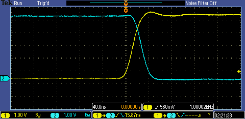 |  |
 |  |
Return to 420L spring 2015
Return to My Labs


