Lab
8 - EE 420L - Characterization of the CD4007 CMOS Transistor Array
Pre-lab work
- Review
the lab write-up.
- Review
the datasheet for the CD4007.pdf CMOS
transistor array.
Introduction
This
lab required us to characterize the transistors (CMOS pairs) in the CD40007 CMOS array.
By measuring our drain current vs a sweeping VGS/VSG or VDS/VSD a few
times along with measuring body effect as we alter VSB/VBS, we can
collect enough data to create a level 1 model in LTSpice (VTO, GAMMA,
KP, TOX) for these transistor. This lab shows us how much different
modeling is verses the real world.
The NMOS
Assuming
that the length of the NMOS is 5 um and its width is 500
um calculate the oxide thickness if Cox (= C'ox*W*L) = 5 pF.
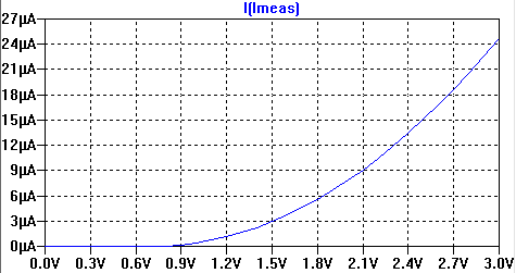
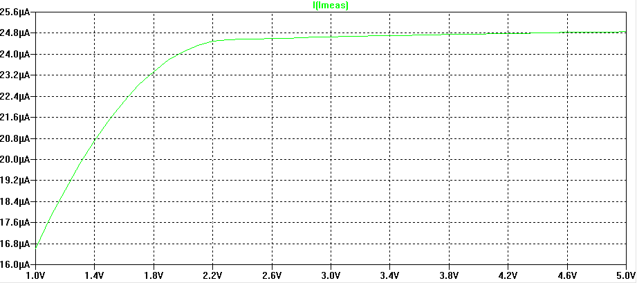
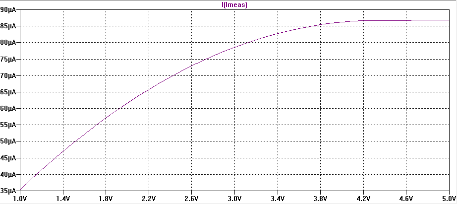
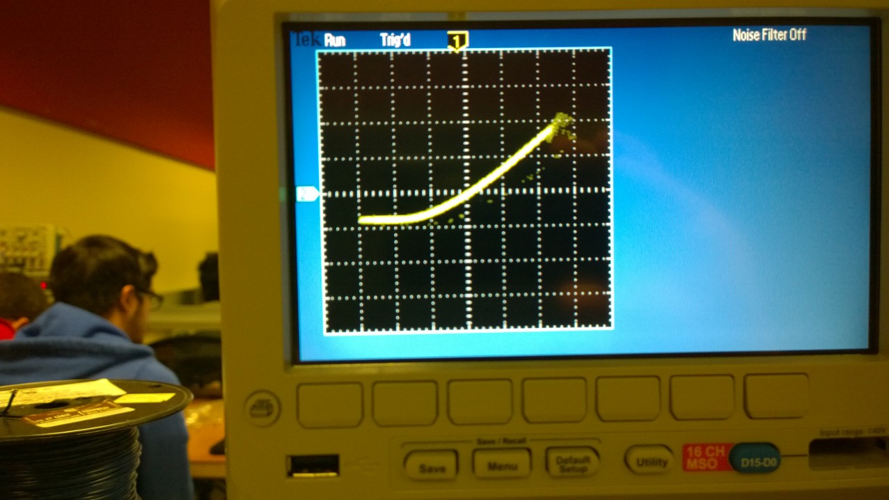
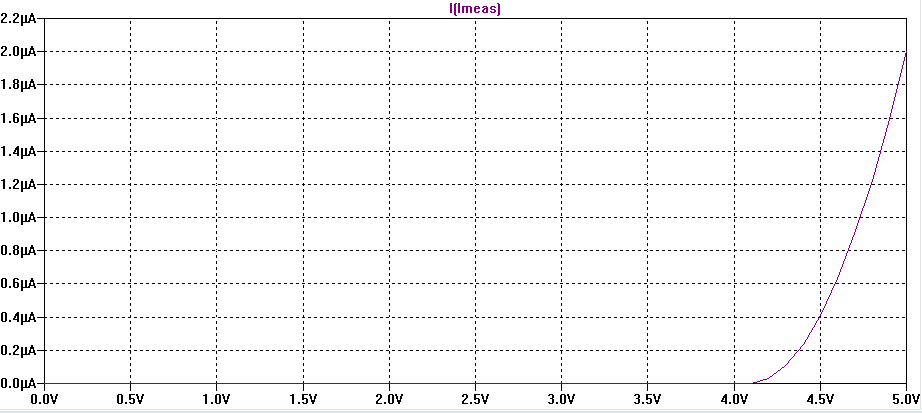
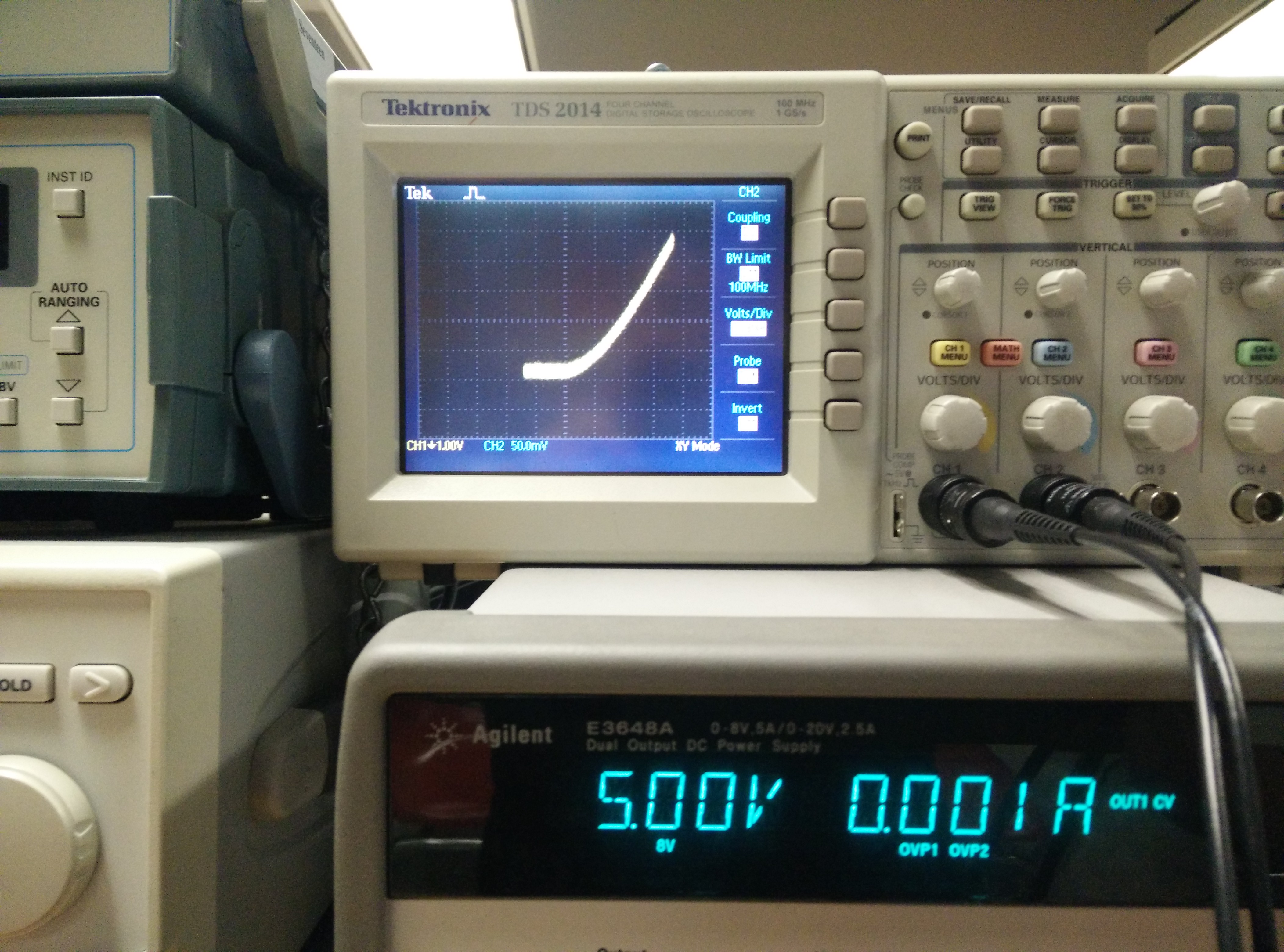
Cox=Cox'*W*L=5pF => Cox'=5p/(5u*500u) = 0.002 Experiment 1: ID v. VGS (0 < VGS < 3 V) with VDS = 3 V

Experiment 2: ID v. VDS (0 < VDS < 5 V) for VGS varying from 1 to 5 V in 1 V steps
VGS = 1V
VGS = 2V
VGS = 3V
VGS = 4V
VGS = 5V
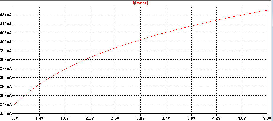
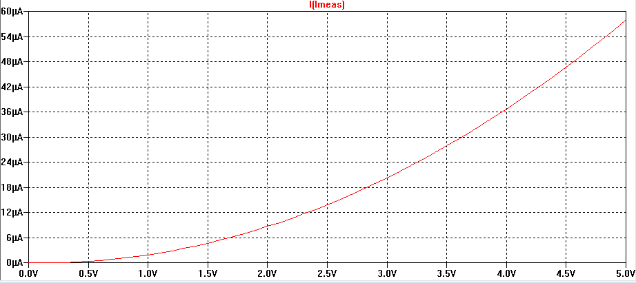
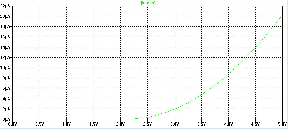
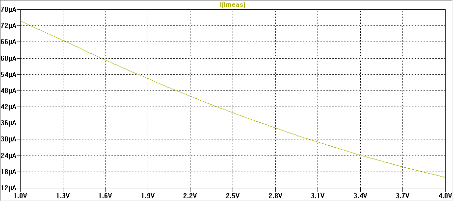
Experiment 3: ID v. VGS (0 < VGS < 5 V) with VDS = 5 V for VSB varying from 0 to 3 V in 1 V steps.
VSB = 0V
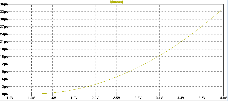
VSB = 1V
VSB = 2V
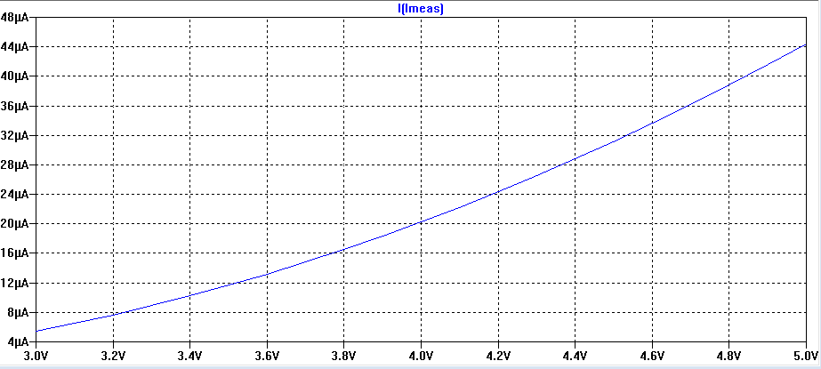
VSB = 3V
The PMOS
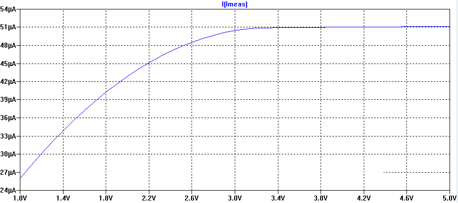
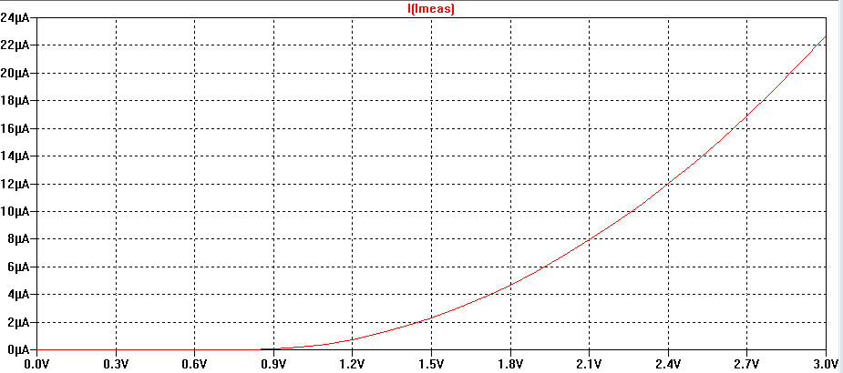
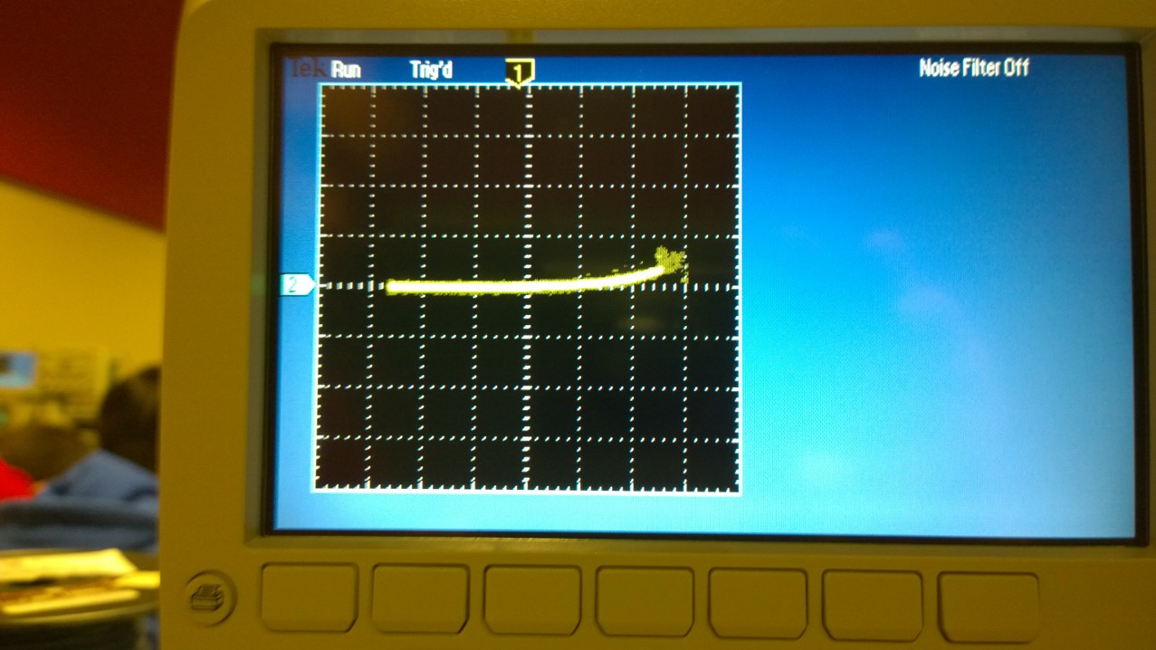
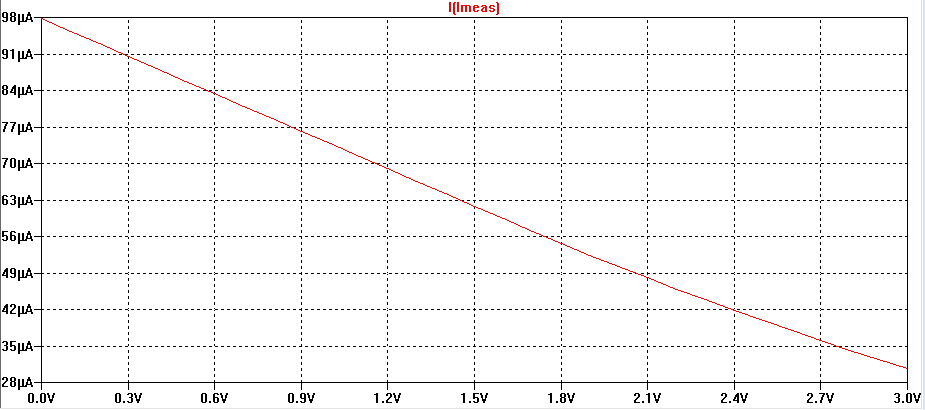
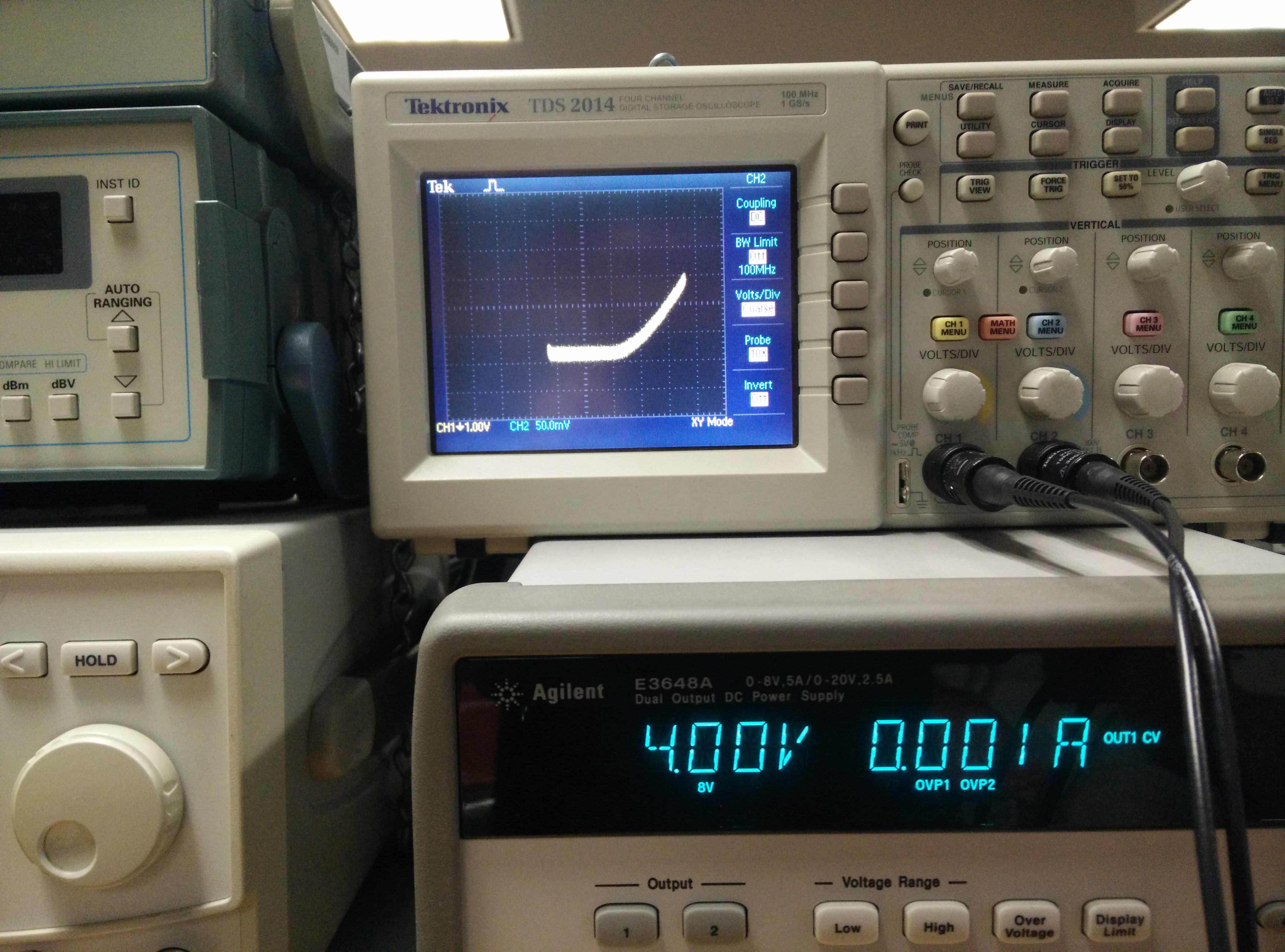
Experiment 1: ID v. VSG (0 < VSG < 3 V) with VSD = 3 V

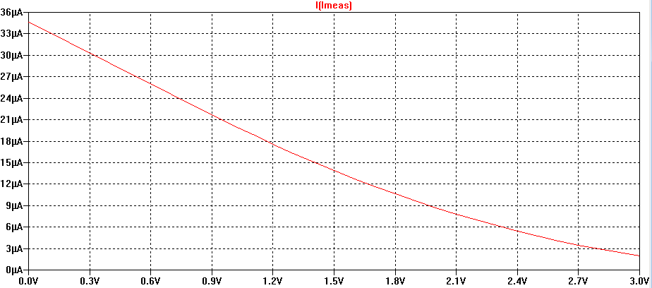
We did not invert our Y axis.
Experiment 2: ID v. VSD (0 < VSD < 5 V) for VSG varying from 1 to 5 V in 1 V steps
VSG = 2V
VSG = 3V
VSG = 4V
VSG = 5V
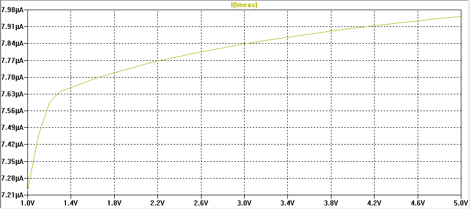
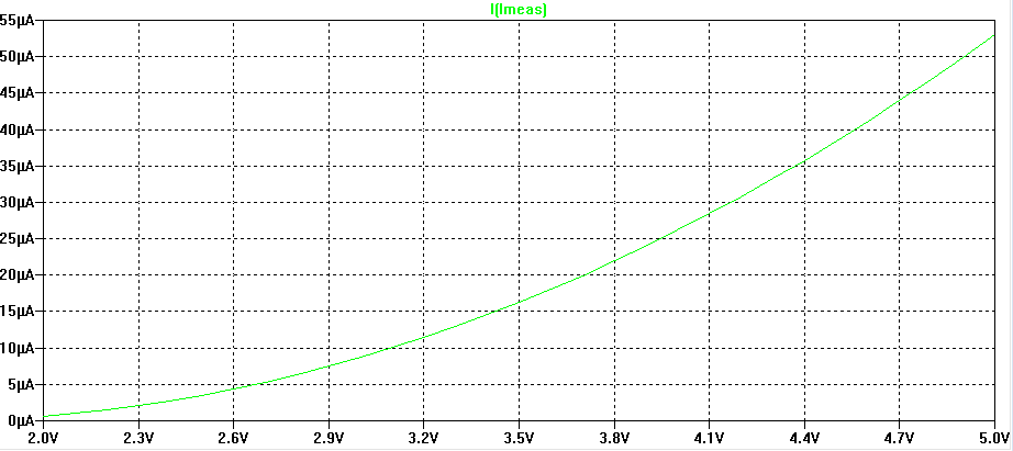
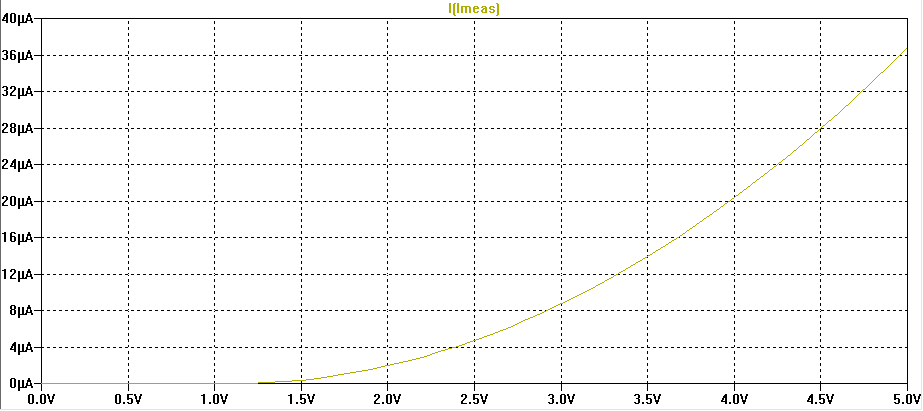
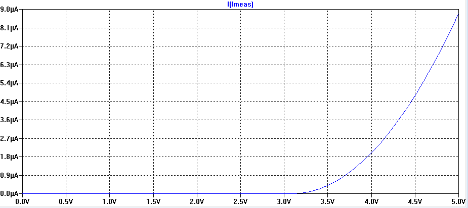
Experiment 3: ID v. VSG (0 < VSG < 5 V) with VSD = 5 V for VBS varying from 0 to 3 V in 1 V steps.
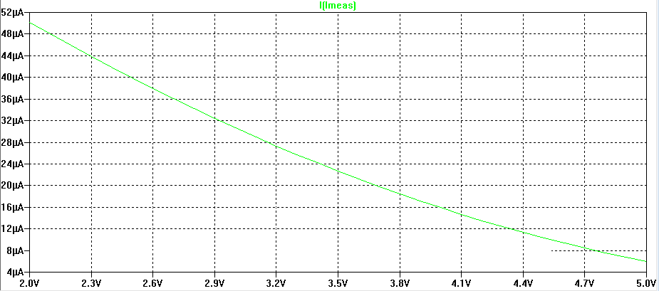
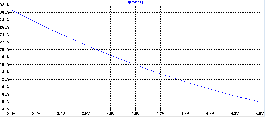
VBS = 3V
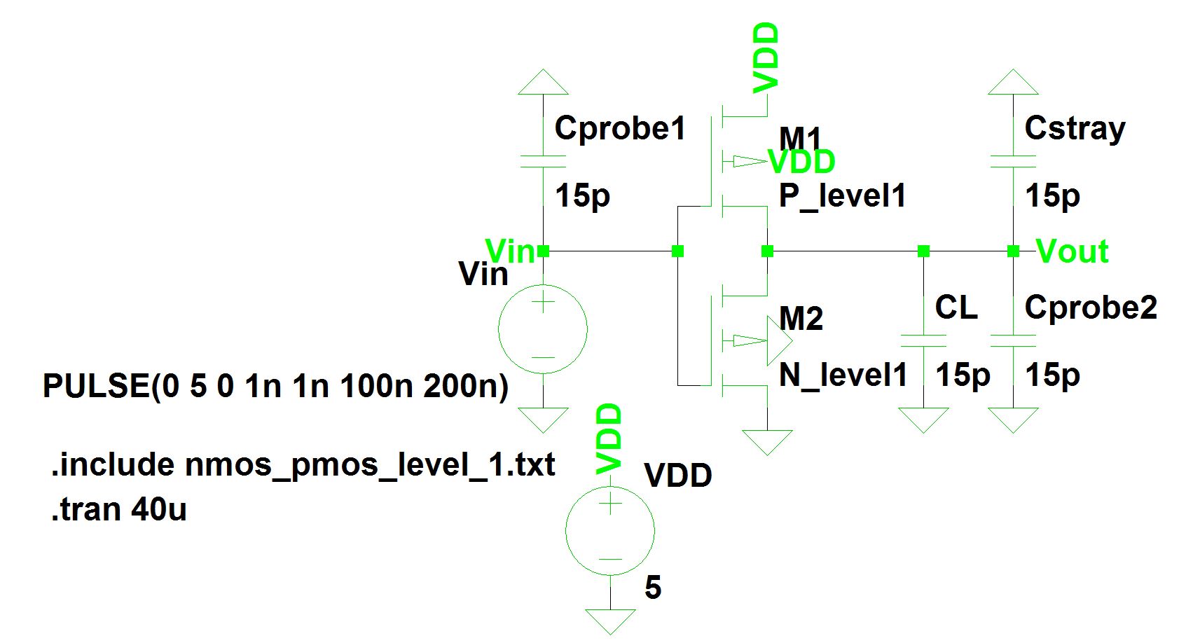
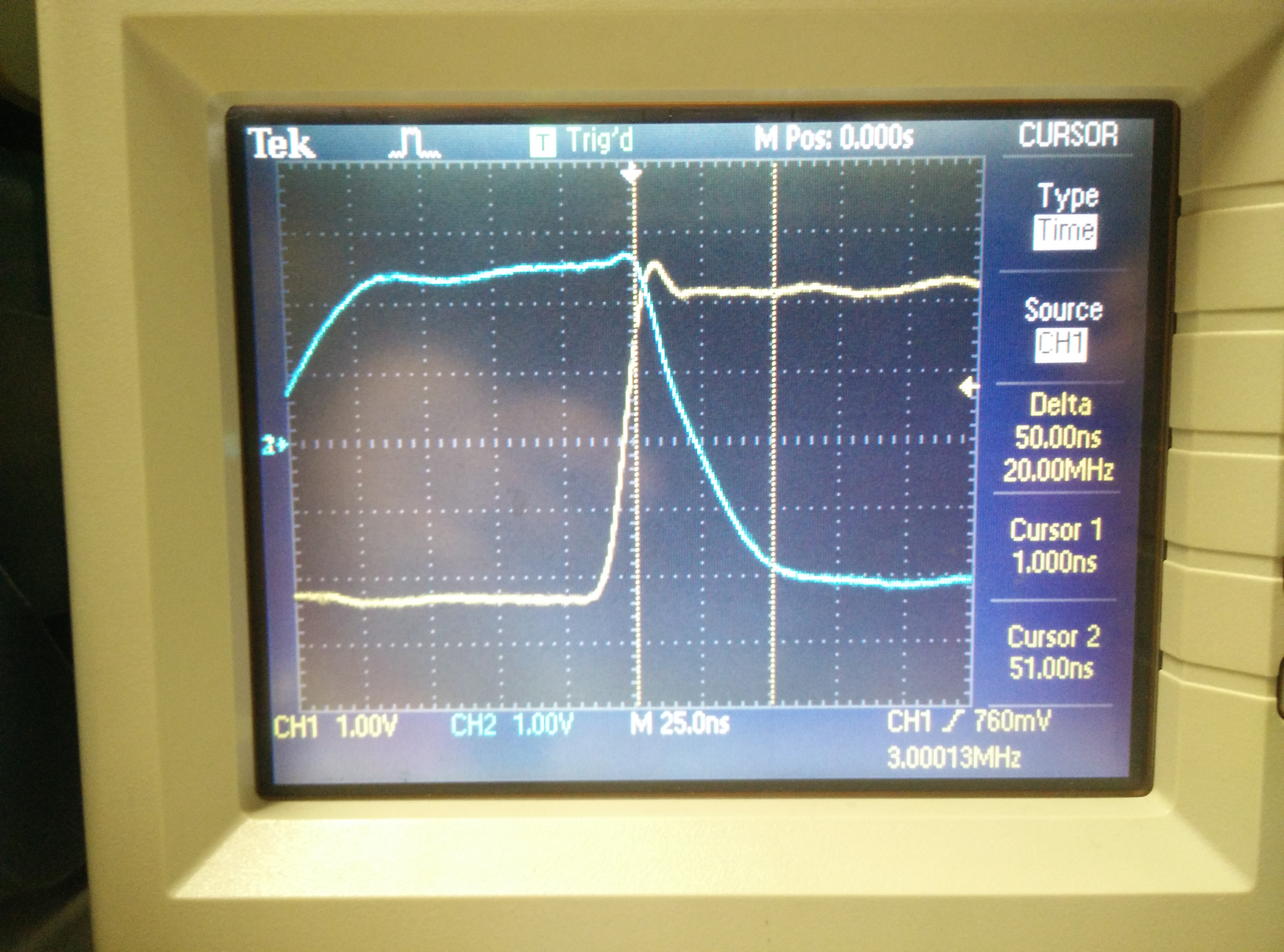
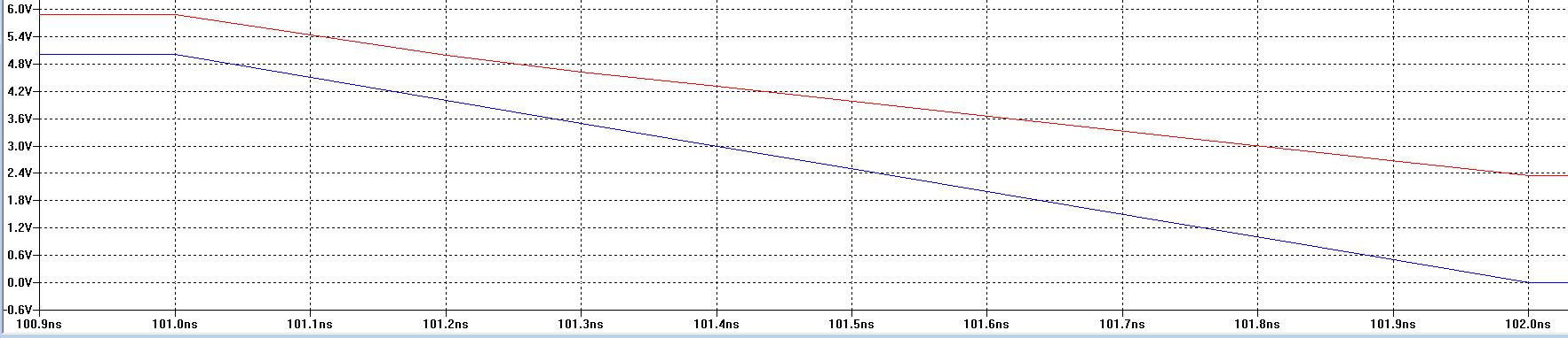
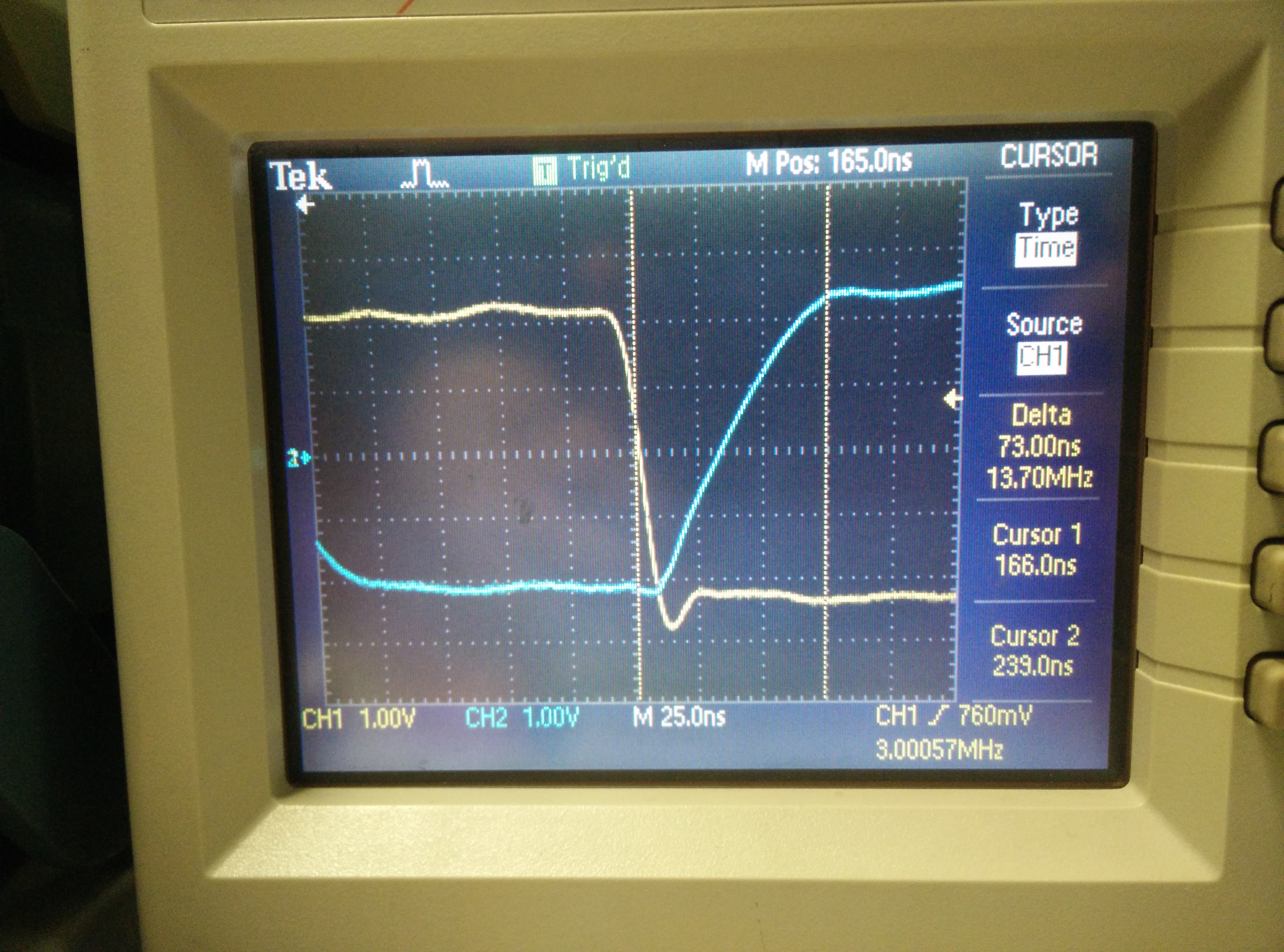
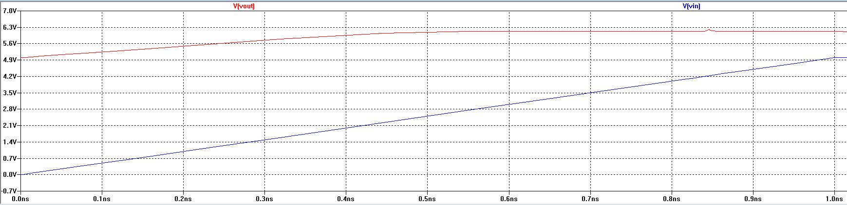
The Inverter
Conclusion
We
created an LTPpice model which has certain similar characteristics from
the transistors we used on the CD4007 chip. The experience from this
lab can be extended to model other chips of transistors and even some
logic circuits if a Spice model is not already created (or if its not
accurate!).
LTspice model:
.MODEL N_level1 NMOS LEVEL = 1
+ TOX = 1.13E-14
+ VTO = 0.8
+ GAMMA = 1
+ KP = 9.38E-6
*
.MODEL P_level1 PMOS LEVEL = 1
+ TOX = 1.13E-14
+ VTO = 0.8
+ GAMMA = 1
+ KP = 4.8E-6
Return
Return to EE420L Student
Directory
Return to EE420L
Page
Return to CMOSedu