Final Project - ECE 420L
Authored
by Nicholas Banas,
Banasn1@unlv.nevada.edu
5/7/15
This lab uses the CD4007 to build a Bandgap Voltage Reference.
BGR Design
Using spice we constructed a BGR out of the CD4007 transistors.
The design uses a self biasing differential amplifier to drive a
pair of mirrored PMOS transistors that drive a PTAT and a CTAT
reference. Due to chip restrictions, limiting the number of
transistors was crucial so the diff-amp is a minimalist design.
BGR:

For the design to work, both R and L needed to be calculated.
The R value controls the branch current and therefor the
value of Vref. Due to the nature of these transistor (detailed in Lab 8) a relatively high branch current of 0.9mA was chosen. To
solve for R:

Next the L was selected to minimize the change in Vref with temperature.

This left us with final values of R1=550 ohms and R2=500ohms.
Design using the CD4007
The CD4007 uses N and PMOS transistors that are interconnected, so
selection of the transistors can be complicated. We made a spice
model using both our calculated transistor models and the modified
models.
Spice model of the CD4007

Using the models, we constructed our circuit and simulated the design.

| Experimental Model | Modified Model |
 |  |
 |  |
Two things are immediately noticeable; the models are do not match well
and the second models show signs of incorrect startup. As the second
model has been generally more accurate, we will continue with it and attempt
to correct the startup.
We do not have
the ability to create the startup circuit described in the textbook, so
a large value resistor will be used. Placing the resistor between
the gate and drain on M7 will bring the gate on M5 up, causing an
imbalance on the diff-amp inputs and starting the circuit. During
normal operation the current through the startup resistor is very small
compared to the currents in the rest of the reference circuit and will
have minimal effect. Here is the corrected modified model
simulation.


The
output now looks as expected for this design. The minimum Vdd is
somewhat larger than I was expecting, Which was Vref + 2Vgs or
around 3.1 volts. Time to build it and see how it really
measures!
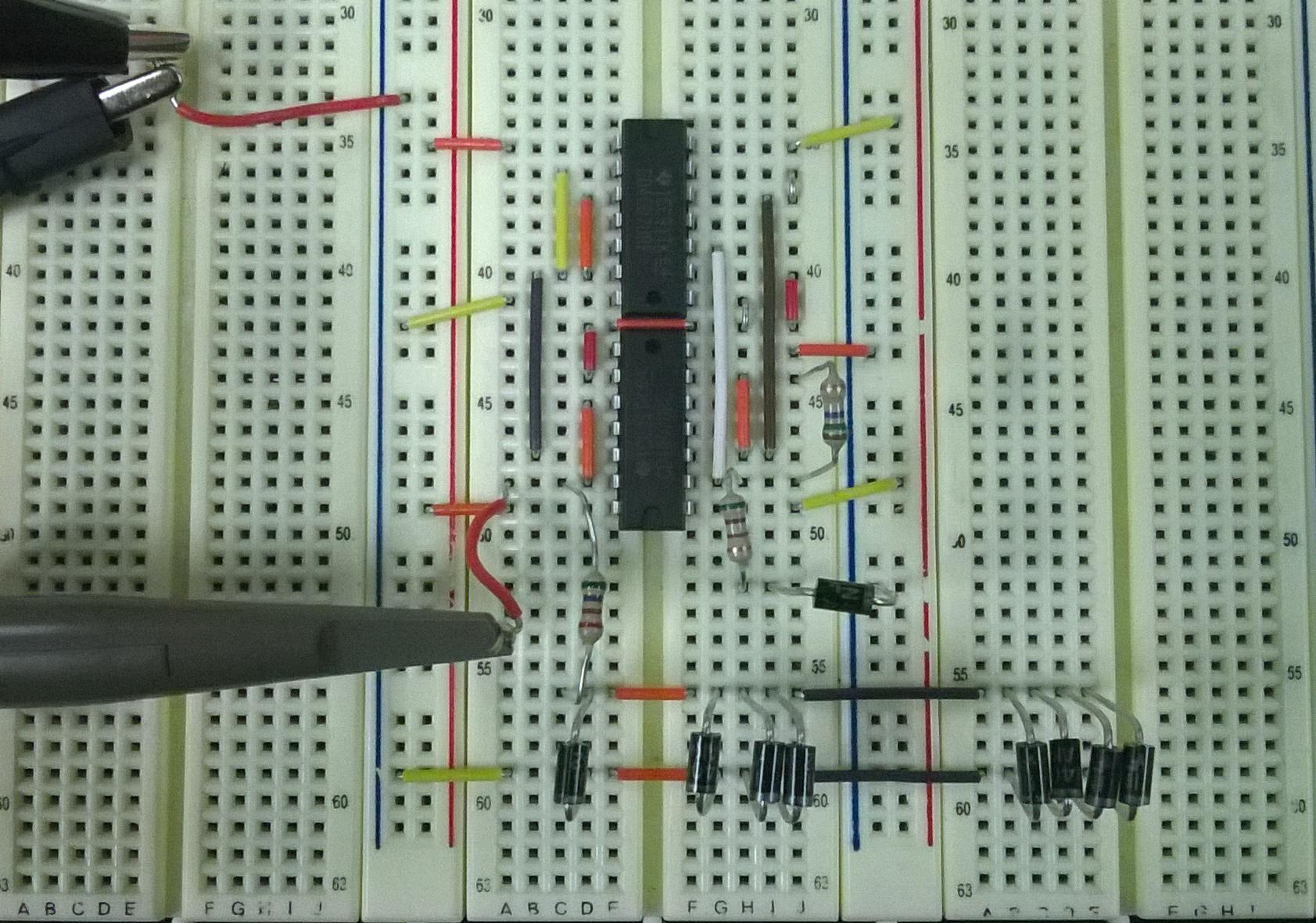
Constructing the BGR
We constructed our BGR using two CD4007's from the same batch on our
breadboard. The 8 Parallel diodes took significant room.
We
measured the voltage at Vref as we swept Vdd from 0 to 10V. As
you can see the measurements are close to the modified model
simulations.
The simulations so 21mV/6.41V ~ 3.3mV/V and the measured results are close to (30mV-10mV)/6V ~ 3.3mV/V.
Temperature Variance
Stepping the temperature we see little variation in the output voltage.
At 0º C the Vref=1.33118V and at 100º
C Vref=1.27007V. This gives us about -61mV/100º C or
-610uV/ºC. This give a TC of -462ppm/ºC not exactly ideal.
Vref traces for 0º C to 100º C

The TC at 5V Vdd

For the physical circuit measurements we took readings at 30º and 80º C
using a heat gun and an instant read thermometer.
The measurements give a value of -20mv/80ºC or a TC of -212ppm/ºC which is somewhat better.
Noise Tolerance
An improvement to the design is to add a moderate capacitor from the
output PMOS gates to VDD. This will increase the tolerance of the
circuit to noise on VDD. Choosing too large of a capacitor will
effect our startup resistor and push the turn on voltage much higher.
We chose a 1nF capacitor for our modeling.

The simulation results show some improvement in the noise on Vref at
the sacrifice of moving the minimum Vdd up by ~.5V.
| No Noise Compensation | Noise Compensation |
 |  |
 |  |
Overall the project seems to be successful. The BGR designed has
a fairly stable output voltage for changes in both Vdd and temperature.


