Lab 6 - EE 420L
Authored
by: WENLAN WU (Stephen)
E-mail: wuw2@unlv.nevada.edu
Date: 4/7/2014
Pre-lab work
1. Review the datasheet of the ZVN3306A and ZVP3306A MOSFETs.
2. Verify the behavior of NMOS and PMOS using the LTspice model in lab6_sims.
3. Watch the video of single_stage_amps and know how to calculate the gain, rin, rout of CS, CF, CG and push-pull opamp.
Lab
description
Lab6 is to build up three types of single stage opamps and calculate and test their gain, rin and rout.
SF: source follower
1. Discuss the DC and AC parameters as talking in video, ID, Vout, vin, vout, AC gain, rin, rout.
2. Use the LTspice to simulate its operation.
3. Build up the circuit and compared to your simulation results and hand calculations.
4.
Talk about how to measure input and output resistance. (PS: Using
electrolitic caps, we need to put the "+" terminal of the cap to the
higher voltage side. Sofor the 10uF input cap, its positive node is connected to gate of MOSFETs.)
CS: common source
1. Discuss the DC and AC parameters as talking in video, ID, Vout, vin, vout, AC gain, rin, rout.
2. Use the LTspice to simulate its operation.
3. Build up the circuit and compared to your simulation results and hand calculations.
4.
Talk about how to measure input and output resistance. (PS: Discuss how
the source resistance Rs, Rsn and Rsp influence the gain.)
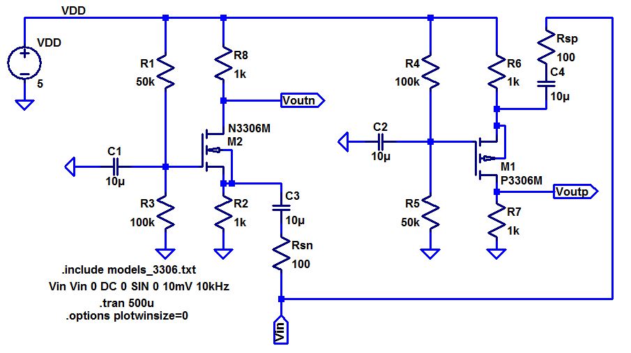
CG: common gate
1. Discuss the DC and AC parameters as talking in video, ID, Vout, vin, vout, AC gain, rin, rout.
2. Use the LTspice to simulate its operation.
3. Build up the circuit and compared to your simulation results and hand calculations.
4.
Talk about how to measure input and output resistance. (PS: Discuss how
the source resistance Rs, Rsn and Rsp influence the gain.)
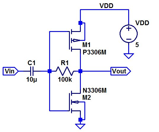
Push-pull opamp
1. Discuss the DC and AC parameters as talking in video, ID, Vout, vin, vout, AC gain, rin, rout.
2. Use the LTspice to simulate its operation.
3. Build up the circuit and compared to your simulation results and hand calculations.
4.
Use the voltage divider to get a smaller input voltage because its gain
is very big. (PS: think about the resistor is replaced by 510k.)
Finally, Don't forget to backup your report and work directory on your computer
or dropbox and upload it to the CMOSedu.com for the future study and
discussion.
Lab6:
Transistor Behavior
For
the NMOS, the drain current will increase after the VGS is bigger than
VTHN. And the slope of the curve Id vs VGS is the transconductance, gm.
Thus the gm will also increase after the VGS is bigger than VTHN. For
Id vs VDS, we know when VDS< VGS-VTHN, the NMOS is in triode region.
Id will linearly inceased by a constant times of VDS. When
VDS>=VGS-VTHN, the drain current will go into saturation region
instead of going up. The NMOS behavior simulation is shown below. Id vs
VGS, Id vs VDS, gm vs VGS.

For the PMOS, the drain
current will increase after the VSG is bigger than |VTHP|. And the slope
of the curve Id vs VSG is the transconductance, gm. Thus the gm will
also increase after the VSG is bigger than |VTHP|. For Id vs VSD, we know
when VSD< VSG-|VTHP|, the PMOS is in triode region. Id will linearly
inceased by a constant times of VSD. When VSD>=VSG-|VTHP|, the drain
current will go into saturation region instead of going up. The PMOS
behavior simulation is shown below. Id vs VSG, Id vs VSD, gm vs VSG.

SF: source follower
1. The following hand calculations shows the DC and AC operations of SF.

2.
First, get the operation points of the circuit. The threshold voltage
of NMOS and PMOS is 1.82V and -2.88V, respectively. The gm of NMOS and
PMOS is 18.3mA/V and 10.7mA/V, respectively.

Use
the simulation model, get the transient of vin, voutn and voutp. We can
see that outputn and outputp are the same as vin. That means both of
them has roughly 1V/V gain.

Simulate the AC analysis from 10kHz to 100kHz. The gain of voutn and voutp is roughly -20dB=1V/V.

Based
on the hand calculations, we know the input resistance is 33k. So we
put the 33k before input capacitor as below. Then we can get the gate
voltage of NMOS and PMOS is half of the input signal.


Based
on the hand
calculations, we also get the output resistance Rout is 55 for
NMOS, 93 for PMOS. So we put the 10uF cap series with 55 ohms resistor
to the output node as below. Then we can get output voltage of
NMOS and PMOS will be half, namely minus 6dB.


3. Build up the circuit and get the experimental results.
For
the experimental design, the input is 100mV@10kHz. From the following
figure, the gain is equal 188m/200m=0.94. It's very close to ideal gain
1 of NMOS.
In
order to measure the input resistance, add the input resistance before
the input cap. Then test the voltage of resisotr two nodes, calculate
the current flows through the added resistance. Thus the input
resistance is the gate voltage(the left node voltage of input cap)
divided by the current.
In
order to measure the output resistance, add the output resistance
series with 10uF to the output ode. Then measure the output voltage and
calcualte the current flows through the added resistance. And also
measure the input voltage on the gate of the MOSFET. Thus the output
resistance is the difference of the input voltage and output voltage
divided by the current.
NMOS Gain

For
the Rin measure, add 33k before the 10uF cap. Then the gate voltage (AC
input voltage) is half of the original one. So the output voltage
should be half. We can see the following result. From the cursor a, b,
we can read the peak to peak value of the output is 120mV, which is
half of the input peak to peak value, 200mV. That means, the 33k
is the input resistance.
NMOS Rin

For
the Rout measure, add 56ohms resistor seires with 10uF cap to the
output node. Measure the output voltage and input voltage on the gate
node. Because
the output resistance is double, so its output voltage should half.
From the following figure, we see that the output voltage is 100mV half
of the input voltage, 200mV. It is proved the output resistance is
56ohms.
NMOS Rout

For
PMOS, the simulation show the gain is 156m/200m=0.78. So that means the
gain is smaller than hand-calculation and the real gm of gm should be
smaller than 10.7mA/V.
PMOS Gain

The
33k input resistance is added. We can see in the following figure,
input and output voltage curve is equal, but the voltage scale of
output is half of that of input. That means, the output voltage is half
of the input. It is proved the input resistance 33k is correct.
PMOS Rin

For
output resistance in PMOS SF, 390ohms resistance has been added and in
the following result, the input and output are just one scale as the
same as the above RIN result. So that means the output voltage is half
of the input, proving the output resistance 390ohms correct.
PMOS Rout

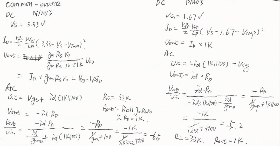
CS: common source
1.
The following hand calculations shows the DC and AC operations of CS.
From the following hand calculation, we see that the source resistance
Rs=1k parallel Rsn=100 or Rsp=100 in the denominator position. That means, if the
Rsn or Rs increased, the gain will decrease.
DC operation
The
dc input is set down by the 50k-100k voltage divider. The dc output is
equal to drain current multiplying the Rd parallel gmRs*ro.
AC operation
The Rin is 100k||50k. The Rout is roughly Rd. The ac gain is the drain impedance divided by the source impedance of MOSFET.
2.
First, get the operation points of the circuit. The threshold voltage
of NMOS and PMOS is 1.82V and -2.88V, respectively. The gm of NMOS and
PMOS is 18.3mA/V and 10.7mA/V, respectively.

Use
the simulation model, get the transient of vin, voutn and voutp. We can
see that outputn is 7 times of vin and outputp is 5 times of vin.

Simulate the AC analysis from 10kHz to 100kHz. The gain of voutn and voutp is roughly 6.8V/V and 5.2V/V.

Based
on the hand calculations, we know the input resistance is 33kohms. So
we
put the 33kohms before input capacitor as below. The outn is 3.4V and
the outp is 2.54V, half of the circuit without 33k oms.


Based
on the hand
calculations, we also get the output resistance Rout is 1k for
NMOS and PMOS. So we put the 10uF cap series with 1k ohms resistor to
the
output node as below. Then we can get output voltage of
NMOS and PMOS will be half, namely minus 6dB.


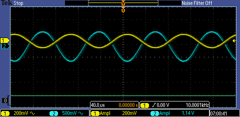
3. Build up the circuit and get the experimental results.
For
the experimental design, the input is 100mV@10kHz. From the following
figure, the gain is equal 1.14/200m=5.7V/V. It's very close to ideal
gain 6.5 of NMOS. And vout has 90 degree phase shift.
NMOS Gain
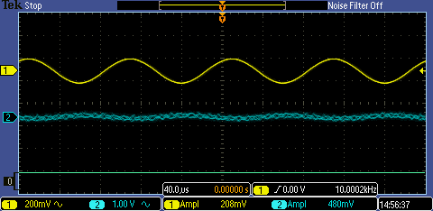
For
the Rin measure, add 33k before the 10uF cap. Then the gate voltage (AC
input voltage) is half of the original one. So the output voltage
should be half. In the following experimental result, the peak to peak value of the output is 600mV, which is
close to half of 1.14V. That means, the 33k is
the input resistance.
NMOS Rin

For the Rout measure, add 1kohms resistor seires with 10uF cap to the output node. Because
the output resistance is double, so its output voltage should half.
From the following figure, we see that the output voltage is 58mV close to half
of 1.14V. It is proved the output resistance is 1k ohms.
NMOS Rout

For PMOS, the simulation show the gain is 480m/200m=4.8V/V.
PMOS Gain

The
33k input resistance is added. We can see in the following figure, The output voltage is close to half
of 480mV. It is proved the input resistance 33k is correct.
PMOS Rin

For
output resistance in PMOS CS, 1kohms resistance has been added and in
the following result the output voltage is close to half
of 480mV, proving the output resistance 1k ohms correct.
PMOS Rout

CG: common gate
1.
The following hand calculations shows the DC and AC operations of CG.
From the following hand calculations, if increasing the source
resistance and Rsn or Rsp the output gain will decrease.
DC operation
As hand calculations, the dc input is set down by R2 voltage. VG is set down by the 50k-100k voltage divider. The dc output voltage is the same as CS.
AC operation
Rin is determined by the Rsn plus RSS||1/gm. Rout is still approximate to Rd. The ac gain is shown below.

2.
First, get the operation points of the circuit. The threshold voltage
of NMOS and PMOS is 1.82V and -2.88V, respectively. The gm of NMOS and
PMOS is 18.3mA/V and 10.7mA/V, respectively.

Use
the simulation model, get the transient of vin, voutn and voutp.
Compared with the CS, CG has the same gain, but doesn't have phase
shift. The voutn is 7 times of vin and voutp is 5 times of vin.

Simulate the AC analysis from 10kHz to 100kHz. The gain of voutn and voutp is roughly 6.1dB and 4.8dB respectively.

Based
on the hand calculations, we know the input resistance of NMOS and PMOS is 155 and 193ohms, respectively. So we
put the 155ohms and 193ohms before input capacitor as below. The gate voltage of MOSFETs are half of the input signal.


The output resistance is the same as CS. So we put the 10uF cap series with 1k ohms resistor to the
output node as below. Then we can get output voltage of
NMOS and PMOS will be half.


3. Build up the circuit and get the experimental results.
For
the experimental design, the input is 100mV@10kHz. From the following
figure, the gain is equal 1.4/200m=7V/V. It's very close to ideal gain 6.5 of NMOS.
NMOS Gain

For
the Rin measure, add 160ohms before the 10uF cap. The output voltage is 640mV close to half of 1.4V. That means, the 33k is
the input resistance.
NMOS Rin

For
the Rout measure, add 1kohms resistor seires with 10uF cap to the
output node. The output voltage is 520mV close to half
of 1.4V. It is proved the output resistance is 1k ohms.
NMOS Rout

For
PMOS, the simulation show the gain is 320m/200m=1.6. So that means the real gm of gm should be
smaller than 10.7mA/V.
PMOS Gain

The 620ohms input resistance is added. The output voltage becomes half
of 320mV. It is proved the input resistance 620omhs is correct.
PMOS Rin

For
output resistance it is also 1kohms. The output voltage also becomes half
of 320mV, proving the output resistance 1k correct.
PMOS Rout

Push-pull opamp
1.
The hand calculations are shown below. From the following gain
equation, increasing RF to 510k can increase the gain 5 times.
DC operation
The
opamp is self-biased. The dc input is equal to dc output because the
big resistor 100k connects them together and no dc current flows in
gate node.
AC operation
The Rin is equal to 100k assuming the gate resistance is infinite. The output impendance is also RF. The ac gain is shown below.

2. In the LTspice simulation, the input amplitude is 1mV @10kHz.
The first result uses RF=100k and its gain is roughly 2k V/V. The
transient analysis shows that the opamp can be pushed to ground but
only pulled to 4.4V instead of VDD. The second uses RF=510k and
its gain is 3.4k V/V instead of 5 times. This is because the output
amplitude can not be pulled above VDD. The transient analysis shows
that output range is from ground to VDD.


3.
In the experimental design, a voltage divider has been used by two
resistors 10k and 10 ohms. The input signal is 100mV@10kHz. The real
input of the opamp is 0.1mV@10kHz. As we expected, if using RF=100k,
the output should be 290mV. The first following figure shows the result
approximate to 290m*2=580mV.
If
using 510k, the output should have 3V*2=6V peak to peak value. The
second figure shows 4.2V, which is reasonable because the real gm is
smaller than what I used in hand calculations.

Summary:
From
above experiments, we study how to calculate gain, rin and rout and how to simulate and measure these parameters.
Backup:
Right
click the mouse to compress the lab6 fold into "lab6.rar". And backup to study folder (e.x. dropbox) or email to myself.
Return to the listing of my labs
Return to the whole class reports
Return to the EE421L
Return to the CMOSedu.com