Lab 4 - EE 420L
For non-inverting op-amp:
1. After watching the video, using the gain-bandwidth product to estimate the BW for non-inverting opamp having gains of 1, 5, and 10.
2. Build up the real circuit to verify these estimations, VCM=2.5V. Show the scope result and discuss any difference between estimations and experimental results.
3. For the final experimental simulatioin result, please show at least four pairs of input and output signal and set input with four different frequencies: @ low frequency, f1 and f2; @f3=f3dB; @f4=fun. The f1 and f2 help show opamp having flat dc gain. The f3 indicates that output signal decreases by increasing the frequency. The fun is the frequency at which |Av|=0dB.
4. It is better to generate a table of output @ different input frequency. And then use the Excel to show the Bode Plot result.
For inversting op-amp
1. After watching the video, using the gain-bandwidth product to estimate the BW for inverting opamp having gains of -1, -5, and -10.
2. Build up the real circuit to verify these estimations, VCM=2.5V. Show the scope result and discuss any difference between estimations and experimental results.
3. For the final experimental simulatioin result, please show at least four pairs of input and output signal and set input with four different frequencies: @ low frequency, f1 and f2; @f3=f3dB; @f4=fun.
4. It is better to generate a table of output @ different input frequency. And then use the Excel to show the Bode Plot result.
Measure the slew-rate of LM324.
1. Use a pusle input to experiment the slew-rate
2. Use a sinewave input to experiment the slew-rate
In your report, please discuss the design and any differences.
Finally, Don't forget to backup your report and work directory on your computer or dropbox and upload it to the CMOSedu.com for the future study and discussion.


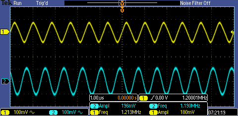
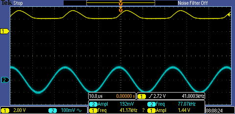
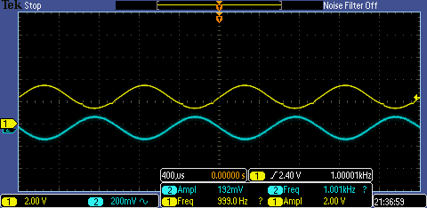
The following figure is the experimental transient result. The output signal is equal to the input signal @1kHz. Due to the datasheet's GBP is at VDD=30V, when we change the VDD to 5V, the GBP will also change. In the unity-gain opamp, I get that when the frequency goes up to 700kHz, the output amplitude starts to reduce. That means the fun=GBP=700k @5V.
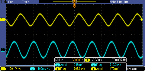
Design the |Av|=5V/V non-inverting op-amp. The LTspice schematic and AC analysis result are shown as below. The measured BW is 388kHz@AV=5V/V.


Now
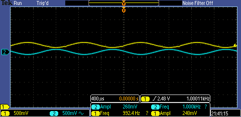
based on the GBP=700k, we build up the second circuit on board. For the
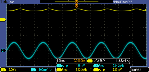
|Av|=5 opamp, its frequency in experiment is supposed to be 140kHz.
That means, at this point, the gain reduced 3dB(|Av|=3.55). Thus if the input amplitude is 200mV, the output amplitude at f3dB is 709mV.
Design the |Av|=10V/V non-inverting op-amp. The LTspice schematic and AC analysis result are shown as below. The measured BW is 162kHz@AV=10V/V.


Also
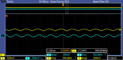
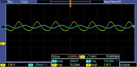
based on the GBP=700k, we build up the third circuit on board. For the
|Av|=10 opamp, its frequency in experiment is supposed to be 70kHz.
That means, at this point, the gain reduced 3dB(|Av|=7). Thus if the
input amplitude is 200mV, the output amplitude at f3dB is 1400mV.


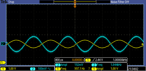
Build up the first inverting opamp. Get the experimental result like the following. The output signal goes down 3dB @500kHz.
Design the Av=-RF/RI=-5V/V inverting op-amp. The LTspice schematic and AC analysis result are shown as below. The measured BW is 315kHz@AV=-5V/V.


Build up the second inverting opamp and get the experimental result like the following. The output signal goes down 3dB @150kHz.
 TEK00016.PNG
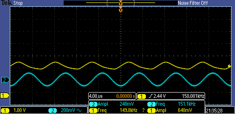
Design the Av=-RF/RI=-10V/V inverting op-amp. The LTspice schematic and AC analysis result are shown as below.The measured BW is 153kHz@AV=-10V/V.


Build up the final inverting opamp and get the experimental result like the following. The output signal goes down 3dB @70kHz.
3. Discussion
Why these BWs from the experimental result is smaller than the BWs from the LTspice models?
1. From the datasheet, we can get the following entry shown the slew rate of LM324.

2. Use a pulse input signal to measure LM324 slew rate. The circuit and simulation result is shown as below. The output from 10% to 90% needs 4.8us. So the SR=(3.2-0.36)/4.8u=0.59V/us.


3. Use a sinewave input signal to measure LM324 slew rate. The circuit and simlation result is shown as below. As discussed in opamp_II video, the input frequency should be not greater than SR/(2*pi*Vo)=4V/us /6.28=63.7kHz. So the input frequency is set as 64kHz and the amplitude is 1. The simulation result shows that the slew rate is exactly 400kV/s=0.4V/us.


4. Discussion
Why the largest output is not 5V, roughly 3.7V, why? And the first SR measured is higher than datasheet value?
From the datasheet, the high level ooutput voltage shown below is 3.5V for VCC=+5V.

Summary:
From above experiments, we study gain-bandwidth product, slew rate. We learned the relationship between frequency, close-loop gain, unity-gain frequency and gain-bandwidth product. Besides, Two methods can be used to measure slew rate.