
Lab 3 - EE 420L
1. Build up the first op-amp1. The VCC+=5V, VCC-=0V.
Define the VCM and discuss VCM influence to an op-amp.
Hand calculate the ideal closed-loop gain.
Discuss the output swing and its center voltage.
Discuss the maximum allowable input signal amplitude. What's more, after increasing the magnitude of the gain to 10, find out the maximum allowable input signal amplitude.
Discuss the 0.01uF capacitor effect. If changing its value, what will happen?
Discuss the input bias current
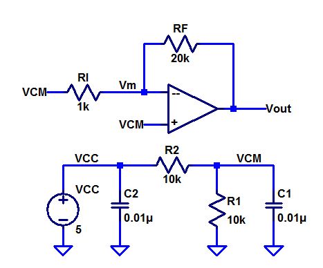
2. Buld up the second op-amp2, which corresponds to the op-amp's offset voltage.
Discuss how to measure the offset voltage.
Discuss the offset voltage after increasing RF to 100k or larger.
Measure the offset voltage of 4 different op-amps and make a comparison.
3. Don't forget to backup your report and work directory on your computer or dropbox and upload it to the CMOSedu.com for the future study and discussion.

2. From the following information capured from datasheet, the good estimation of LM324's open-loop gain is 100dB.


3. The good esimation of input offset is 5mV. The worse case design, we should use 9mV.

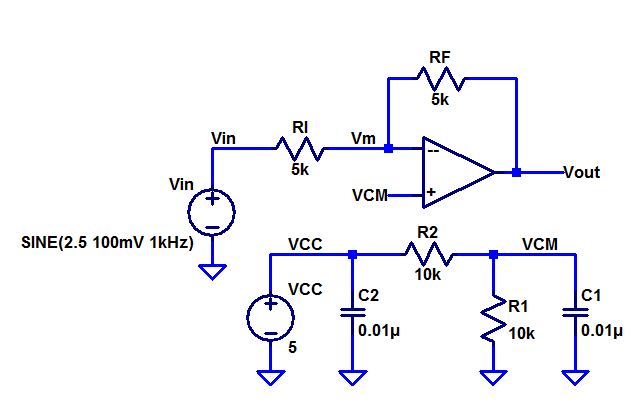
1. The first opamp schematic is shown blow. Its VCM equals to 2.5V without changing. Because in opamp1, the VCM is generated by the 10k voltage divider, which is DC voltage. The following transient curve proves VCM without changing. After watching Dr.Baker's opamp_I video, we can calculate the ideal open-loop gain is -RF/RI=-1=0dB. The output signal has 180 phase shift compared to Vin.


2. The output signal centered at 2.5V and has a swing from 2.4V to 2.6V. If the DC voltage of input is larger than 2.5V, the output center voltage will go down. Otherwise, the DC voltage of output will go up. Because (Vin-VCM)/RI=(VCM-Vout)/RF, so increasing Vin leads Vout reduction.


3. Because the maximum VCM is 3.5V, so the maximum allowable input amplitude is 3.5-2.5=1V @ Av=0dB. Too larger or two smaller input amplitude leads the input MOSFETs moving into triode region affecting the output swing and open-loop gian. The corresponding output will have overshoot or undershoot. If the magnitude of the gain is increased to 10, the maximum of input amplitude will be divided by 10.
The first figure in the following shows that @Av=0dB, the amplitude of input increases from 0 to 2V. The second one shows that @Av=10, the amplitude of input increases from 0 to 200mV.


4. The 0.01uF capacitors connected VCC and VCM to ground are the decoupling capacitors, which is used to make them stable. Increasing the capacitance doesn't affect the DC voltage value of VCM and VCC, but it needs more space increasing the chip cost.
5. Disuccs the Input bias current (IBC) and Input offset current(IOC)

The IBC is the average of the currents into the two input terminals with the output at a specified level. From the entry of electrical characteristics table in the datasheet, the IIB = 20nA. The following reference is from TI Understanding Op Amp Parameters. And also we can read the the Opamp tutorial from AD.
The IOC is the difference between the currents into the two input terminals with the output at the specified level. In LM324, the IIO=2nA.

6. The second opamp is shown as below. Two inputs are connected to VCM. If the opamp is ideal with zero offset, there is no current flowing through RI and RF. So Vout should be equal to Vm and VCM. Simulate and check the Vout result, its difference from VCM is the offset voltage. We also need to use the model to measure 4 different op-amps as shown below. From the operating points, dividing Vout, Vout1, Vout2, Vout3 by VCM is the offset voltage, respectively.


Summary:
From above experiments, we study some parameters: opamp input range, output swing, common-mode voltage, offset voltage, input bias current, input offset current and open-loop gain, etc.
