Lab 8 - EE 420L
Authored
by Worku, Yetneberk
E-mail: workuy@unlv.nevada.edu
Today's
date 04/29/14
Pre-lab work
1. Review the datasheet of the CD4007 CMOS transistor array.
2.
Understand, how the bodies of the NMOS are tied to pin7 (VSS, generally
the lowest potential in the circuit, say ground) and the bodies of the
PMOS are tied to pin 14 (VDD, generally the highest potential in the
circuit, say +5V).
Lab description
A.
Lab 8 will characterize the transistors in the CD4007 and generate
Level1=1 SPICE models. In other words, don't characterize the devices
at higher than +5V or lower than ground potential.
B. Experimentally generate both NMOS and PMOS device , then plots of
- ID v. VGS (0 < VGS < 3 V) with VDS = 3 V
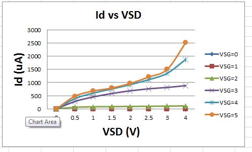
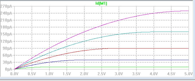
- ID v. VDS (0 < VDS < 5 V) for VGS varying from 1 to 5 V in 1 V steps, and
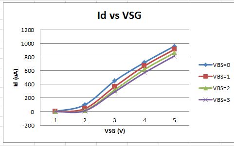
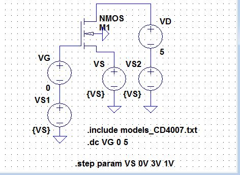
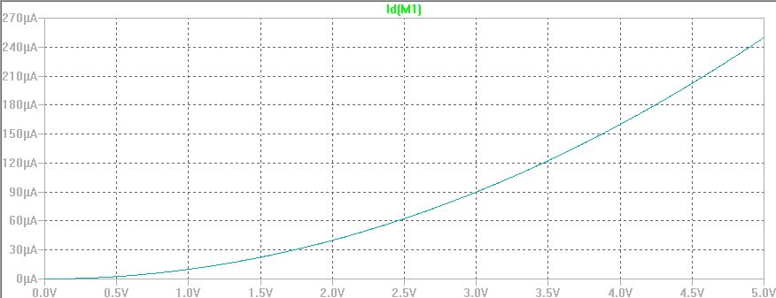
- ID v. VGS (0 < VGS < 5 V) with VDS = 5 V for VSB varying from 0 to 3 V in 1 V steps.
C.
Assuming that the length of the NMOS is 5um and its width is 500
um calculate the oxide thickness if Cox (= C'ox*W*L) = 5 pF
D. From this measured data create a level = 1 MOSFET model with (only) parameters: VTO, GAMMA, KP, and TOX.
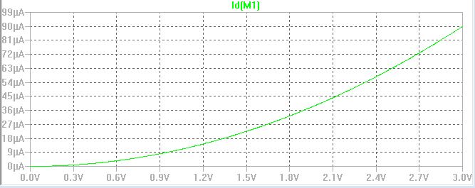
E. Use the spice model to generate the above current voltage curves.
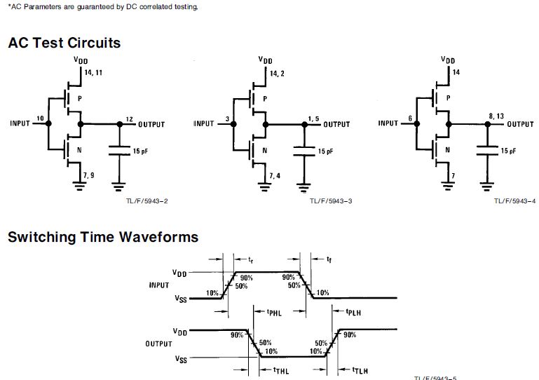
F. Finding rising and falling time, also testing propagation delay from low to high, tPLH and from high to low, t PHL.
G.
Simulate the delays and compare to the measured results with LTspice
model. Adjust the SPICE model to get the better matching between
measured data and simulation data
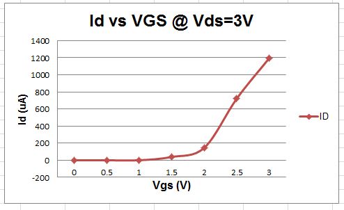
NMOS : Id vs VGS @ VDS =3V
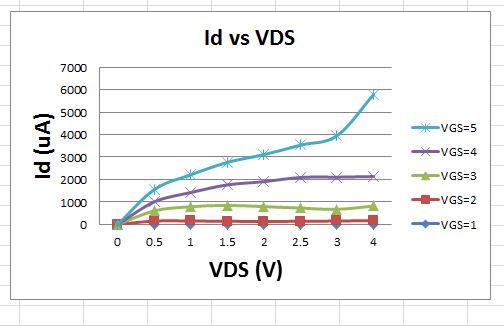
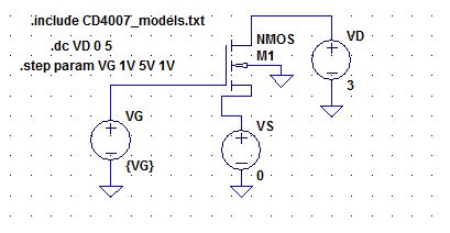
NMOS : Id vs VDS @ changing VGS from 0 to 5
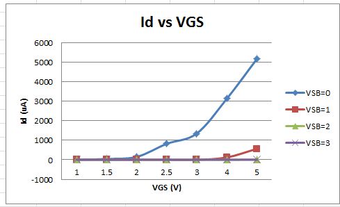
NMOS :Id vs VGS @ changing VSB from 0 to 3V
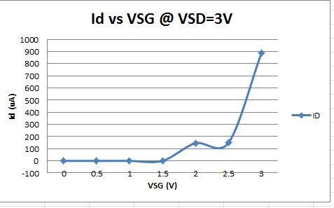
PMOS: Id vs VSG @ VSD=3V
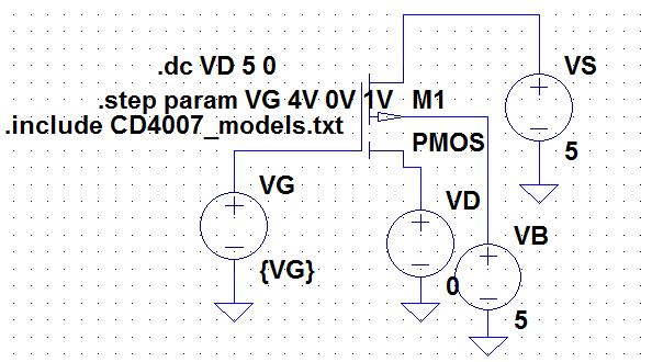
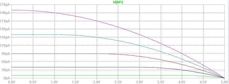
PMOS ; Id vs VSD @ changing VSG FROM 0 TOI 5V
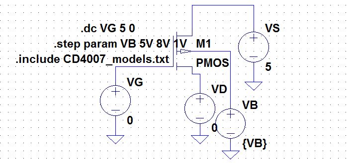
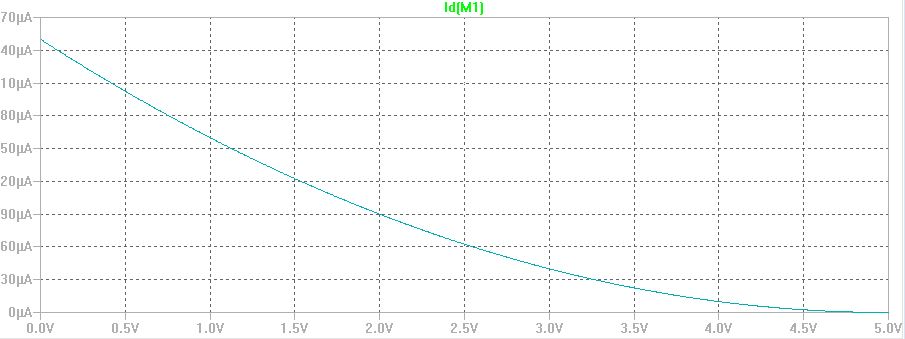
PMOS : Ed vs @ changing VBS from 0 to 3V
1. Assume L=5u, W=500u, and Cox=5p. Also, TOX = eox/C'ox=3.98*8.78e^-16/(COX/WL) = 17.6*10^-12m
KPn = 2*Id/(VDS,SAT)^2 = 3rd Id vs VDS= 200E^-10, KPp = 2*Id/(VSD,SAT)^2 = 3rd Id vs VSD= E40^-10,
VTO: based on the 3rd ID vs VSD (VDS) results, for NMOS is 1V and PMOS is 1.5V
GAMMA(V1/2): To find Gamma first find Ro, 1/Ro=change Id/change VDS, then Gamma = 1/Ro*Id,sat; NMOS IS .5, and PMOS is .6
3. Generating three I-Vcurves of NMOS/PMOS, based on calcultions
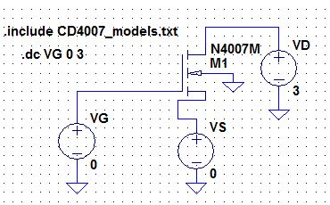
4. showing LTspice circuits in waveform
NMOS
NMOS : Id vs VGS @ VDS =3V
NMOS : Id vs VDS @ changing VGS from 0 to 5
NMOS :Id vs VGS @ changing VSB from 0 to 3V
PMOS: Id vs VSG @ VSD=3V
PMOS ; Id vs VSD @ changing VSG FROM 0 TOI 5V
MOS : Ed vs @ changing VBS from 0 to 3V
The delay of an inverter , the following AC test circuit is found on the third page of the datasheet .
Indeed, the expected result have some slide different from lab experiments, however we studies how to design an audio apamp.
Here is the model: CMOSEDU_MODELS.txt
Return to the listing of my labs
Return to the whole class reports
Return to the EE421L
Return to the CMOSedu.com