Lab 6 - EE 420L
Authored
by Worku, Yetneberk
E-mail: workuy@unlv.nevada.edu
Today's
date 04/16/14
Op-amps III, the op-amp integrator
Pre-lab work
A. Wach the video of single_stage_amps provided on line and know how to calculate the Gain, Rin, Rout each circuit.
B. Provid Hand calculations and compare it with LTspice to simulation result and bulild up the circuit results.
Lab Description and Goals:
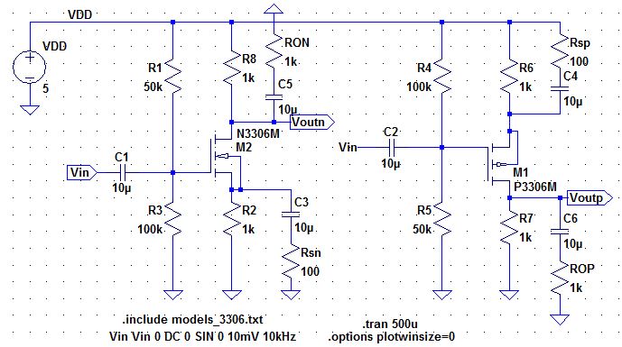
Lab 6 build up source follower, common source, common gate, and push-pull opamp and test their Gain, Rin, Rout.
SF: source follower
1. Build up the circuit and find DC and AC parameters, then compare it with simulation resulats and hand calculations
CS: common source
1. Build up the circuit and find DC and AC parameters, then compare it with simulation resulats and hand calculations
CG: common gate
1. Build up the circuit and find DC and AC parameters, then coampare it with simulation resulats and hand calculations.
Push-pull apamp
1. Build
up the circuit and compare it with simulation results and hand
calculations, however we will use the voltae divider to get a smaller
input voltage.
Lab 6:
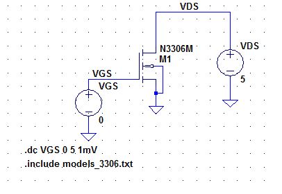
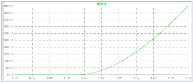
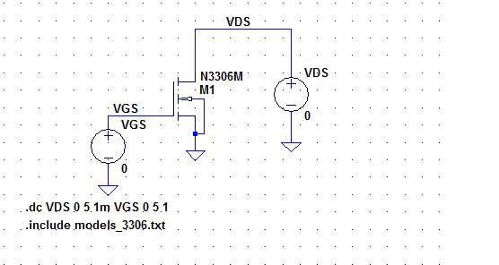
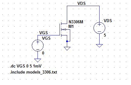
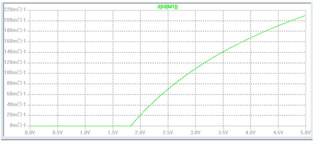
Transistor Behavior
The drain current, and gm will increase after the VGS > VTHN
For the NMOS behavior simulation is shown below Id vs VGS, Id vs VDS and gm vs VGS
 As
such, a voltage divider using a 10k resistor and a 10ohm resistor is
used to reduce the AC input voltage. This is shown below:
As
such, a voltage divider using a 10k resistor and a 10ohm resistor is
used to reduce the AC input voltage. This is shown below: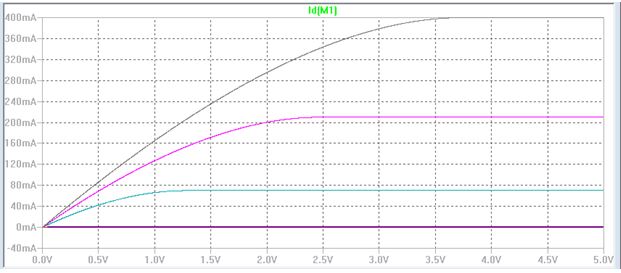
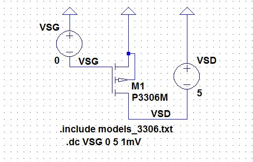
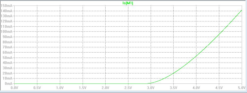
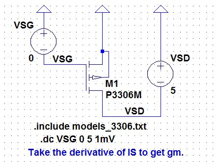
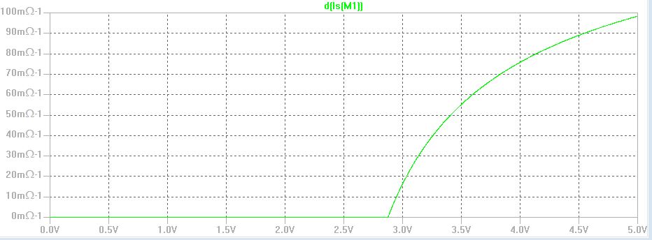
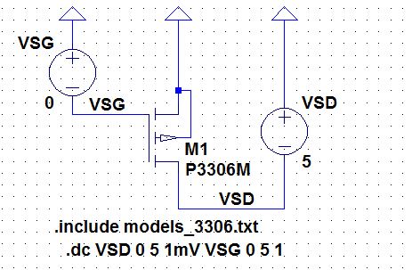
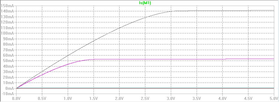
For
the PMOS, the drain current and gm will increase when VGS > |VTHP|.
When VSD>= VSD-|VTHP then Id will linearly increased, also the Id vs
VSG, Id vs VSD, and gm vs VSG showing below the behavior simulation on
PMOS.
SF: source follower
1. the following hand calculations shows the DC and AC operations of SF
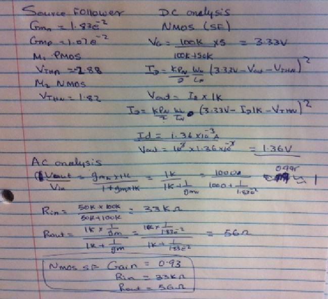
2.
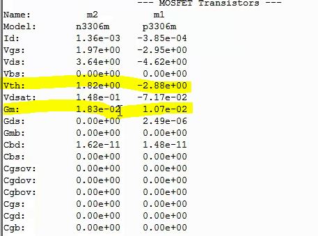
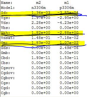
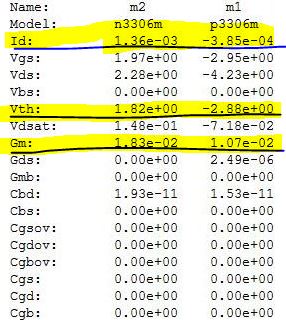
The threshold voltage of NMOS and PMOS is 1.82V and -2.88V
respectively. The gm of NMOS and PMOS IS 18.3Ma/v AND 10.7mA/V
respectively.
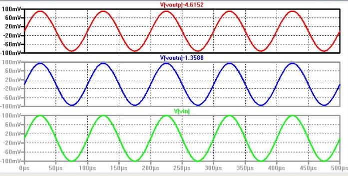
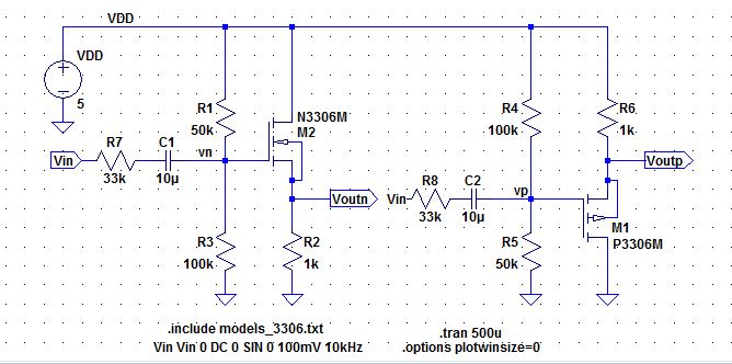
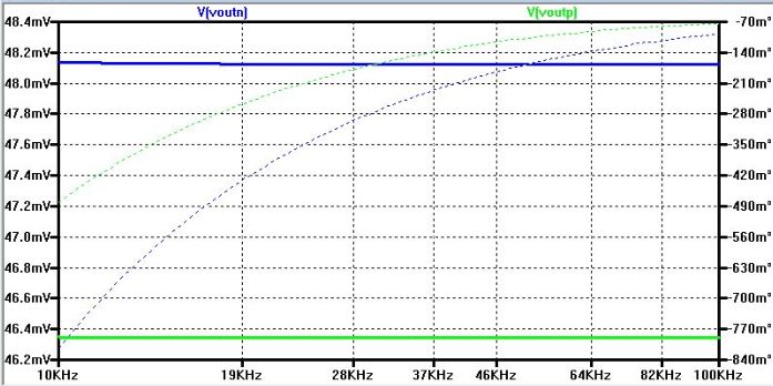
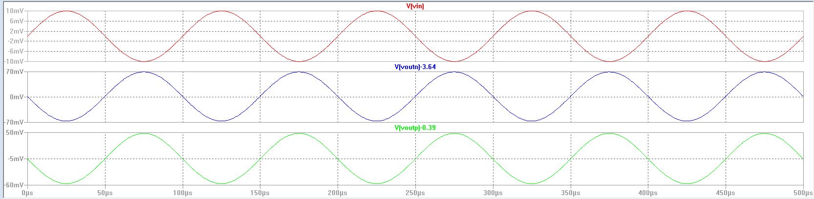
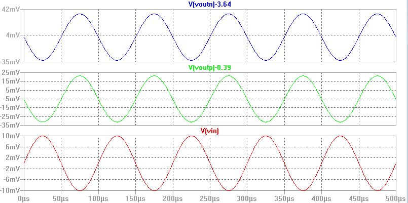
The LTspice showing below the transient of Vin, Voutn and Voutp are the same, because both of them has almost 1V/V
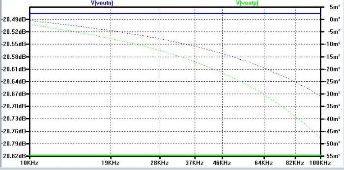
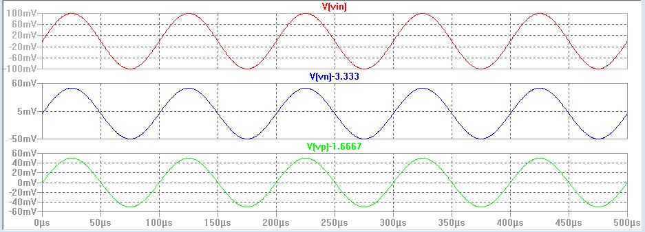
AC analysis from 10kHz to 100kHz, the Gain is almost -20dB=1V/V
Based
on the hand calculations, putting the 33k before input capacitor as
below, we can get half of the input signal NMOS and PMOS.
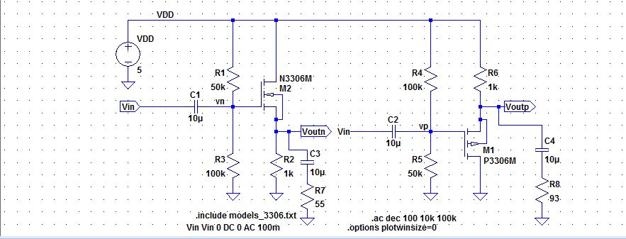
Based on the hand calculation, Rout is 56
for NMOS 93 for PMOS. also, we put 10uF cap in series with 56
ohms resistor, so we can get half of output voltage. simulations is
showing below.
3. Buil up the circuit and get the experimental results
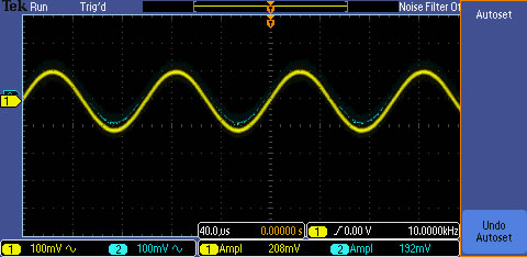
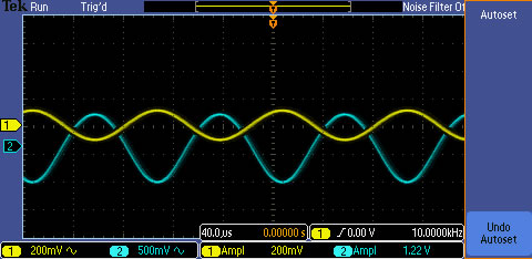
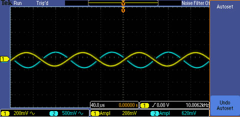
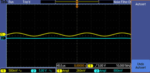
For the experimental design, the input is 100mV@10kHz. Gain is 192m/200m=0.96. It is very close to ideal gain 1 of NMOS.
Measuring
Rin, add input resistance before the input cap, and measuring Rout ,
add the output resistance series with 10uF to the output node. however,
the ouput resistance is the difference of the input voltage and output
voltage divided by the current.
NMOS Gain
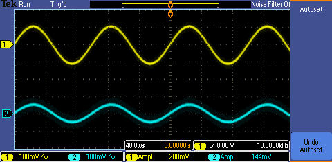
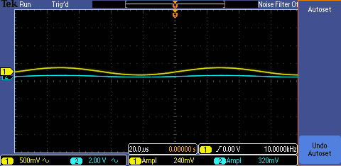
For the Rin measure , add 33k before the 10uF cap. AC the gate voltage is half of the original one.
NMOS Rin
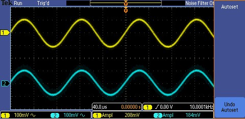
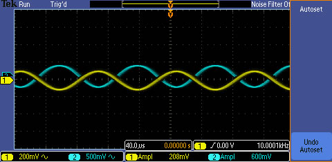
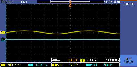
For the Rout measure add 56ohms resistor seires with 10uF cap to the ouput node, so the output voltage should be half.
NMOS Rout

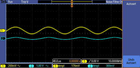
For PMOS, the simulation show the gain is as follolws
PMOS Gain
PMOS Rout
CS: common source
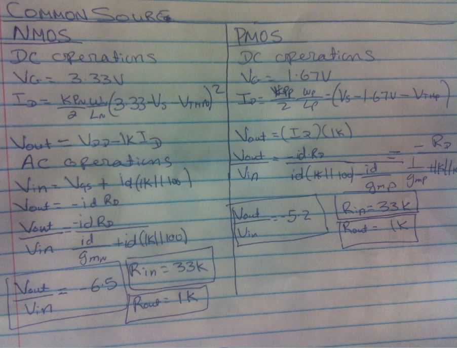
1.
The following hand calculations shows the AC and DC operation of the
common Source amplifier. when the Rsn or Rsp increasing the gain will
decrease because of Rsn and Rsp are in the demominator.
2.
The threshold voltage of NMOS is 1.82V, and the threshold votage of
PMOS is -2.88V. also, th gm value of NMOS is 18.3mA/V, and the gm
value of PMOS is 10.7mA/V
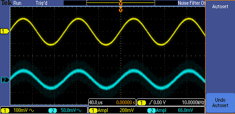
now can be see form simulation model the gain of outputn is 7 times of vin and outputp is 5 times of vin.
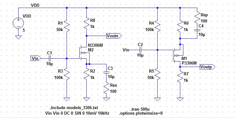
According
to the hand calculations, Rout is 1k for NMOS and PMOS. So we put
the 10uF cap series with 1k ohms resistor to the output node as below.
Then we can get output voltage of NMOS and PMOS will be half,
3. The experimental results are shown below.
According to the lab results the gain is equal to Vout/Vin =1.22V/200m = 6.10V/V
NMOS Gain
To get Rin replacing 33k before the 10uF cap. So the output voltage should be half.
NMOS Rin
To get Rout add
1kohms resistor seires with 10uF cap to the output node. Because the
output resistance is double, so its output voltage should half. From
the following figure, we see that the output voltage is 600mV close to
half of 1.22V. It is proved the output resistance is 1k ohms.
NMOS Rout
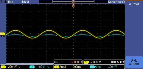
To get PMOS Gain, the simulation show the gain is 320m/200m = 3.2V/V
PMOS Gain
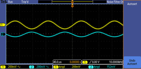
The
33k input resistance is added.; then the output voltage is close to
half of 320mV. It is proved the input resistance 33k is correct.
PMOS Rin
For PMOS 1kohms resistance has been added and the resuslt output voltage is half of 320mV
PMOS Rout
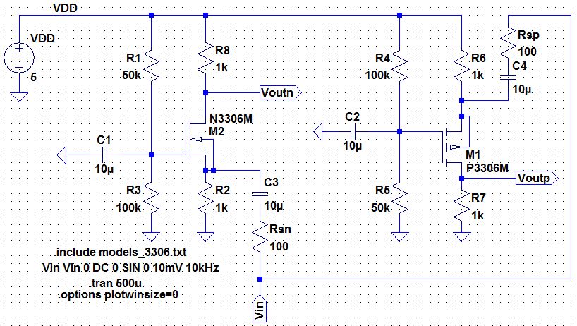
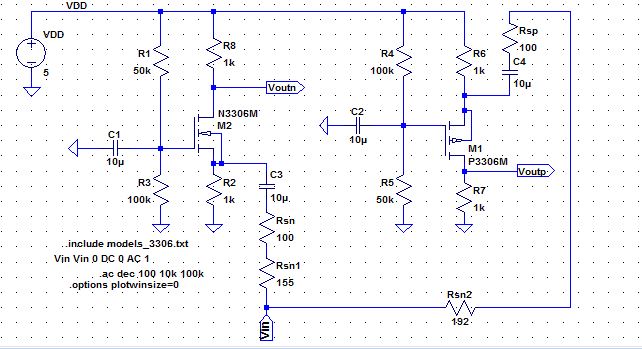
CG: common gate
1. the following hand calculations illustrate the DC and AC operatiions of CG. When the Rsn or Rsp increasing the gain will decrease.
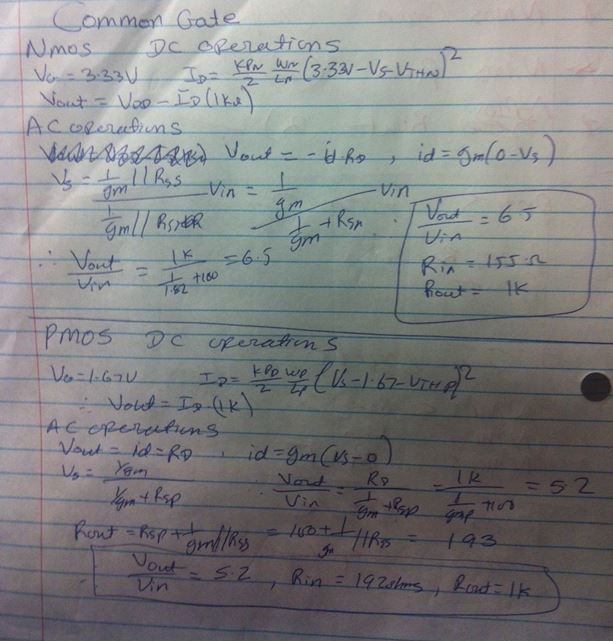
2. The threshold voltage of NMOS is 1.82V, and the threshold votage of
PMOS is -2.88V. also, th gm value of NMOS is 18.3mA/V, and the gm
value of PMOS is 10.7mA/V
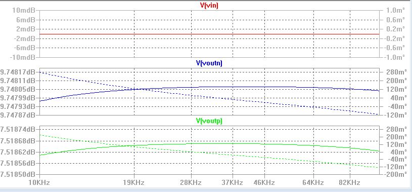
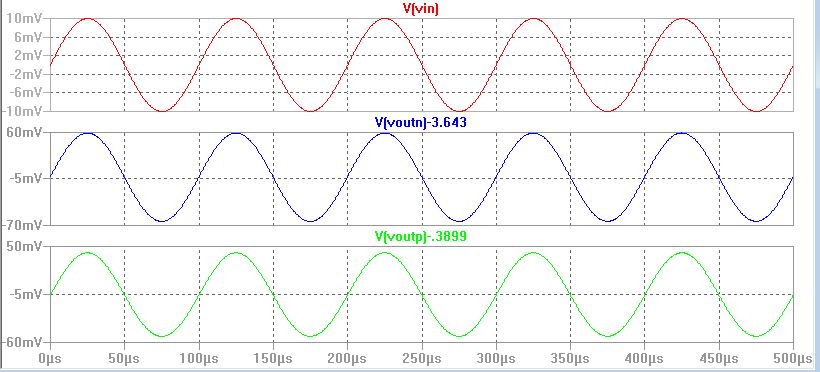
To
get the result of simulation model, use transient of vin, voutn and
voutp. Compared with the CS, CG has the same gain, but doesn't have
phase shift. The voutn is 7 times of vin and voutp is 5 times of vin.
From
hand calculations, we know that input resistance of NMOS and PMOS are
155 and 192ohms respectively.replacing 155 and 192ohms before input
capacitor showing below, therefore, gate voltage of mosfet are half of
the input signal.
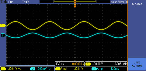
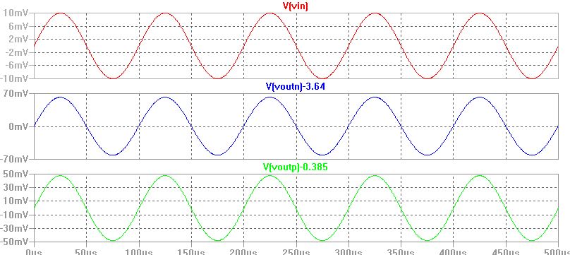
3. The experimentsal results are shown below, however the input is 100mV@10kHz. the gain is equal 800m/200m=4V/V. NMOS Gain
To get Rin can be add 160ohms before the 10uF cap.
NMOS Rin
To get Rout can be add 1kohms resistor seires with 10uF cap to the output node.
NMOS Rout
For PMOS the gain is 360m/200m=1.8. So that means the real gm of gm should be smaller than 10.7mA/V.
PMOS Gain
The
620ohms input resistance is added. The output voltage becomes half of
360mV. It is proved the input resistance 620omhs is correct.
PMOS Rin

To
get output resistance it is also 1kohms. The output voltage also
becomes half of 360mV, proving the output resistance 1k correct.
PMOS Rout
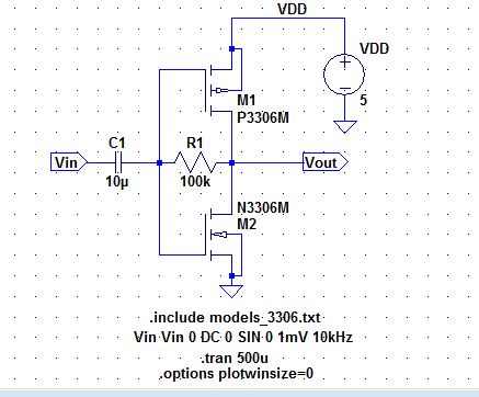
Push-pull opamp
1. The following hand calculations shows below then from gain equation increasing RF to 510k can increase the gain 5.
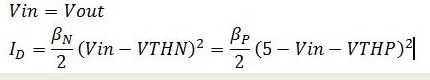
Vin = Vout
The ouput impendance is also RF. the ac agin is shown below
push-pull
Vout = Vin - RF(gmp +gmn) = -100k(16.3m +10.7m) = -2900
2. LTspice simulation, and schematic results are showing below.
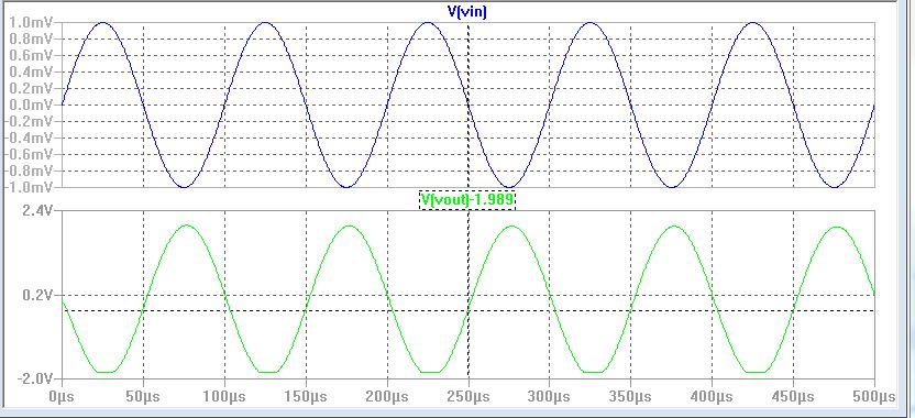
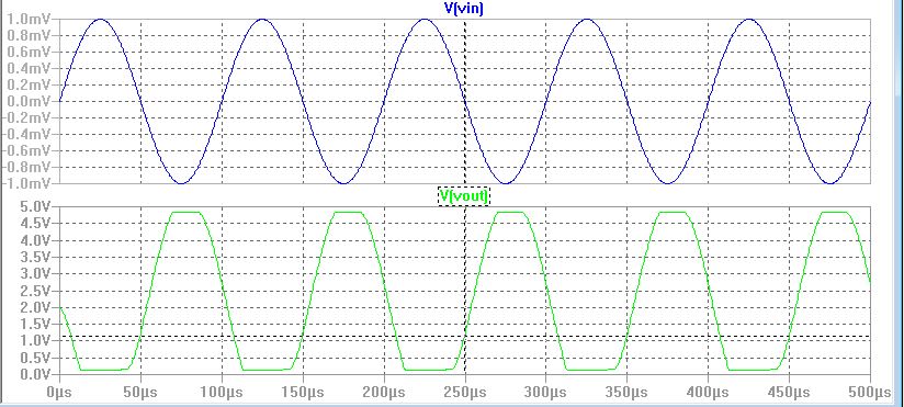
for a 1.0mV input a 2.0V output is generated
the following waveform changed by repelacing R1 to 510k
As such, a voltage divider using a 10k resistor and a 10ohm resistor is used to reduce the AC input voltage.
Vout = Vin (10/10m +10) = 0.1mV
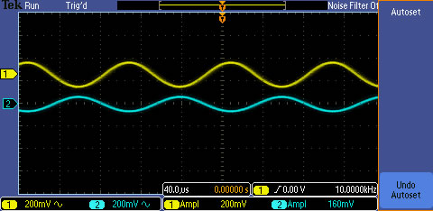
3. The experimentsal results are shown below, by using RF = 100k, and the input voltage to the amplifer is 0.1mV
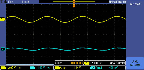
vout/vin=400mv/0.2mv = 2000v/v
Indeed,
the expected result have some slide different from lab experiments,
however we studies how to calcultat gain, rin and rout.
Add
a return to the listing of your labs
Return to the listing of my labs
Return to the whole class reports
Return to the EE421L
Return to the CMOSedu.com