Lab 4 - EE 420L
Authored
by Worku, Yetneberk
E-mail: workuy@unlv.nevada.edu
Today's
date 03/15/14
Pre-lab work:
1. Watch the video op-amps II, review op-amps II notes, and simulate the circuits given.
2. read data sheet of LM324 amplifier, and write up provided on the website.
Lab Description:
1. Estimate, using he datasheet, the bandwidths for non-inverting op-amp topologies having gains of 1, 5, and 10.
2.
Experimentally verify these estimates assuming a common-mode voltage of
2.5V, also discuss any difference between experimental, and estimated
results.
3. Report should provide schematics of the topologies we
are using for experimental verification along with scope
pictures/results.
4. Repeat these above steps using the inverting
op-amp topology having of -1, -5, and -10, also design two
circuits for measuring the slew-rate of the LM324. One circuit should
use a pulse input while the other should use a sine wave input; then,
moment on any differences between measurements and the
datasheet's specifications.
Non-inverting op-amp.
1.
Build
up the real circuit in lab, and using the SPICE model in LTspice. Using
the gain-bandwidth product to estimate the BW for non-inverting
op-amp having gain of 1, 5, 10.
2. Gain bandwidth product
(GBP) = gain (Av)* bandwidth (BW). The gain bandwidth product of the
LM324 showing on datasheet is as follow.

3. When the Gain is 1, 5, 10 then BW is 1.3MHz, 260KHz, 130KHz respectively.
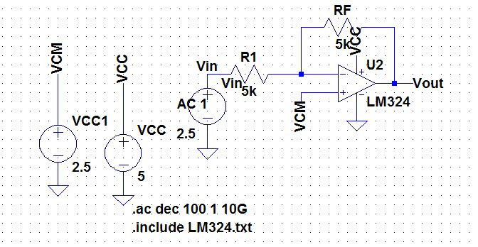
The
following non-inverting amplifier in lab experiment was created as
follows R1 set to 1k and R2 set to 4k to get the correct value for
the gain. Gain = Av= [1 + (R2/R1)] . to show BW readings performed at different frequency
such as 1Hz, 10Hz, 100Hz 1kHz, 10kHz, 100kHz, and 1G.
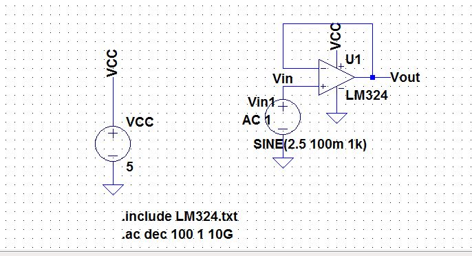
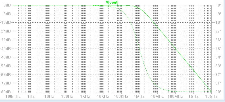
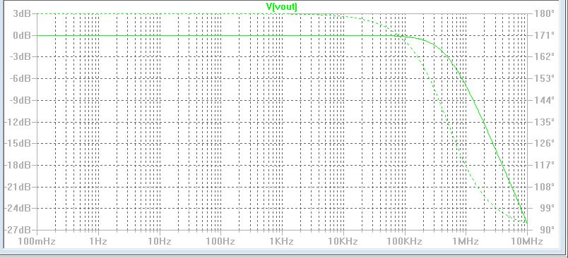
When the gain |Av| is = 1V/V, the LTspice schematic and AC analysis result are shown as below.
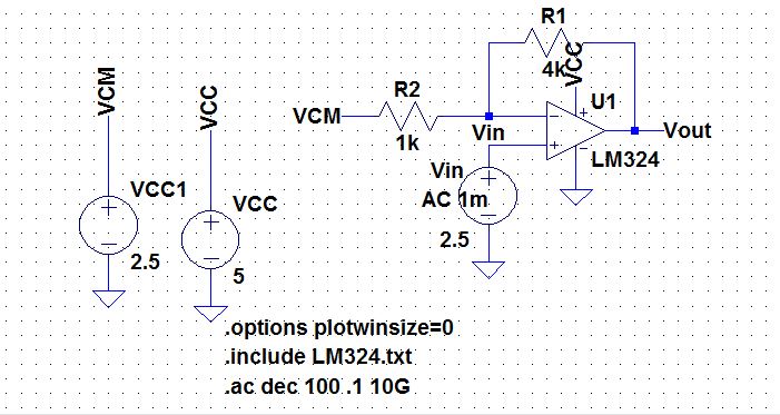
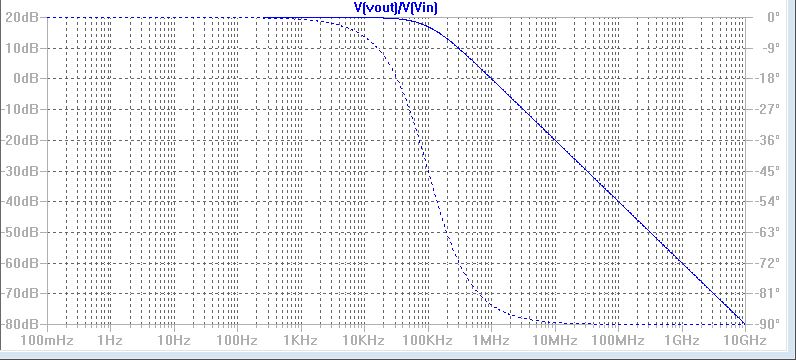
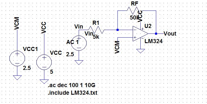
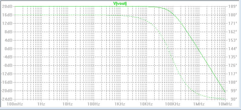
When the gain is |Av| = 5V/V, the LTspice schematic and AC analysis result are shown as below.
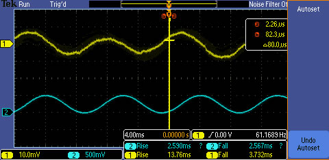
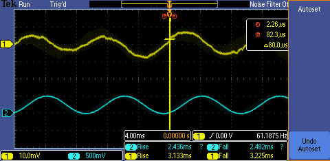
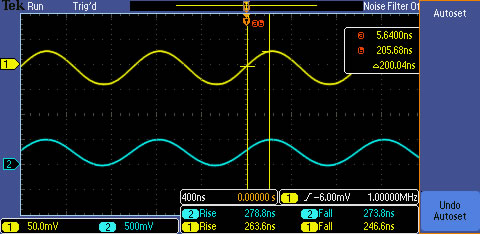
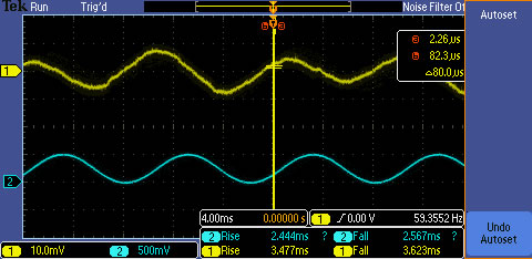
In Lab experiment, when the gain is |Av| = 5V/V then to perform BW at different frequencies,
such as 1Hz, 10Hz, 100Hz 1kHz, 10kHz, 100kHz, and 1G. Also input is yellow color and the output is blue color.


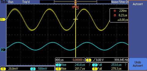
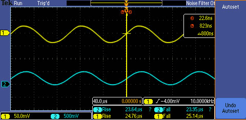
When the gain is |Av| = 10V/V, the LTspice schematic and AC analysis result are shown as below.
In Lab experiment, when the gain is |Av| = 10V/V then to perform BW at different frequencies,
such as 10Hz, 100Hz 1kHz, 10kHz, and 100kHz. Also input is yellow color and the output is blue color.


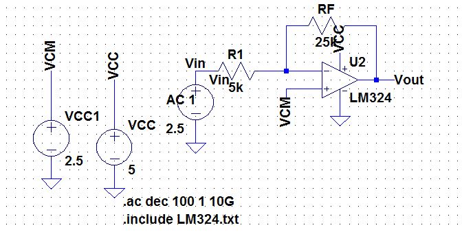
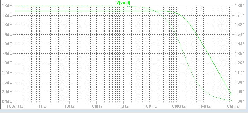
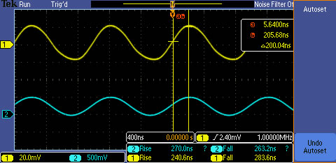
When the gain is |Av| = -1V/V, the LTspice schematic and AC analysis result are shown as below.
In Lab experiment, when the gain is |Av| = -1V/V then to perform BW at different frequencies,
such as 10Hz, 100Hz 1kHz, 10kHz, and 100kHz. Also input is yellow color and the output is blue color.


When
the gain is |Av| = -5V/V, the LTspice schematic and AC analysis result are shown as below.
In Lab experiment, when the gain is |Av| = -5V/V then to perform BW at different frequencies,
such as 10Hz, 100Hz 1kHz, 10kHz, 100KHz and 1MHz. Also input is yellow color and the output is blue color.


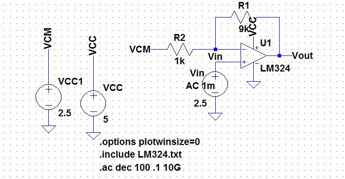
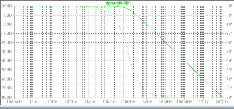
When
the gain is |Av| = -10 the LTspice schematic and AC analysis result are shown as below.
In Lab experiment, when the gain is |Av| = -10V/V then to perform BW at different frequencies,
such as 10Hz, 100Hz 1kHz, 10kHz, 100KHz and 1MHz. Also input is yellow color and the output is blue color.
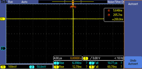


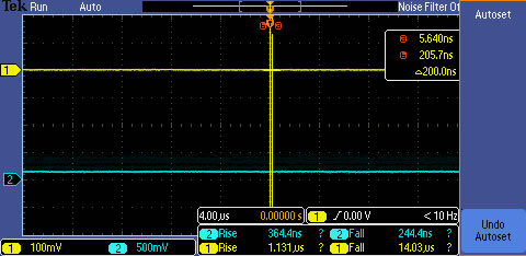
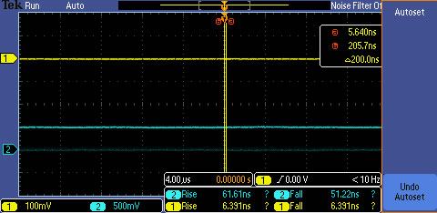
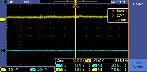
measure slew rate
A. The slew rate is given from datasheet as 0.4V/us.

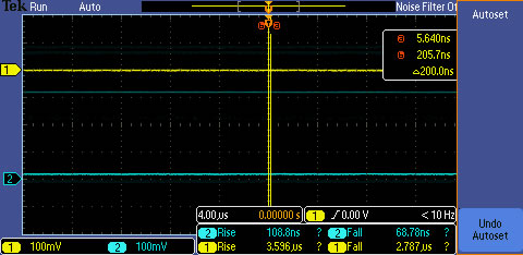
The
output from 10% to 90% needs 5.44us, so the SR=(4.99-1.25)/5.44u =
0.68V/us. also the circuit and simulation result is shown as below
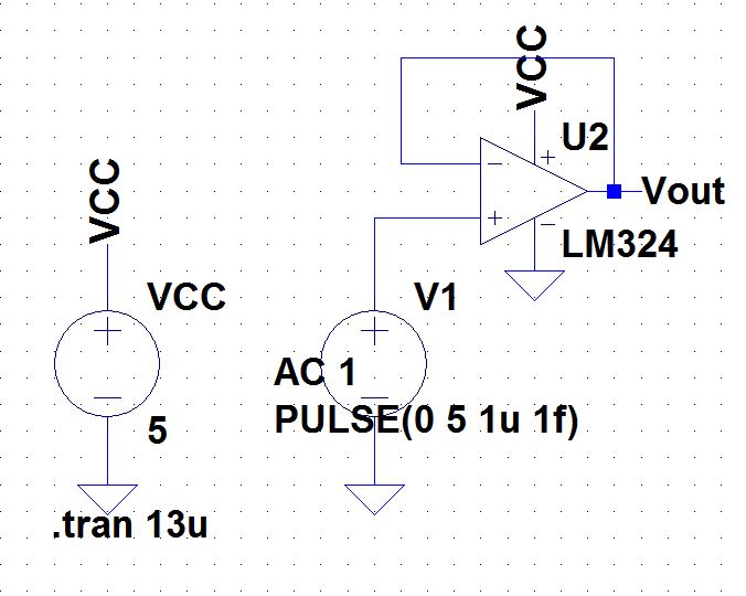
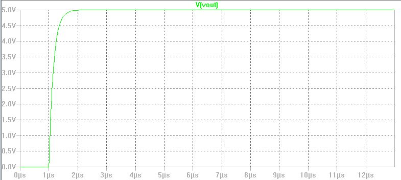
for the first experiment in pulse singal was inputed into the 0p-amp
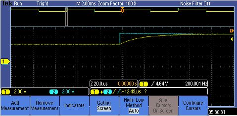
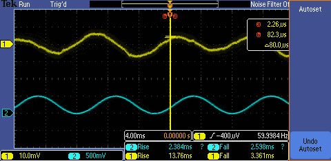
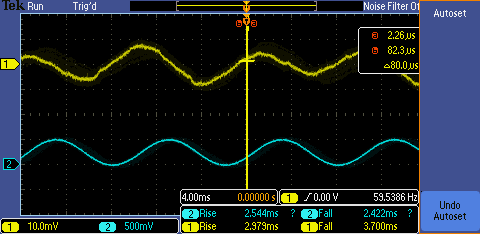
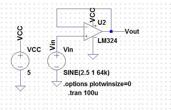
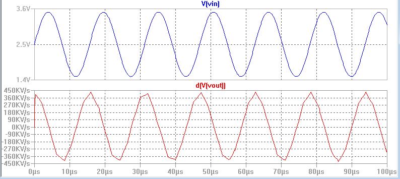
B. The
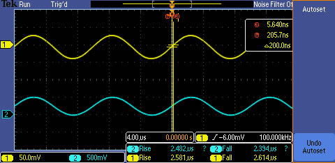
circuit and simlation result is shown as below. the input frequency
should be not greater than SR/(2*pi*Vo)=4V/us /6.28=63.7kHz. So
the input frequency is set as 64kHz and the amplitude is 1. The
simulation result shows that the slew rate is exactly 400kV/s=0.4V/us.
Indeed,
the expected result have some slide different from lab experiments,
however we studies how to measure slew rate, gain-bandwidth product,
BW, and frequency.
Add
a return to the listing of your labs
Return to the listing of my labs
Return to the whole class reports
Return to the EE421L
Return to the CMOSedu.com