Lab X - ECE 421L
Lab description:
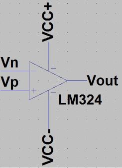
>> Build up the first and second op-amp.1. for the forllowing questions and experiments assume VCC+ = +5V and VCC- = 0V.
A. knowing the non-inverting input, Vp, is at the same potential as the inverting input, Vm, (called the common-mode voltage, VCM) what are the maximum and minimum allowable common-mode voltage?
:- The Minimum VCM, and The Maximum VCM at 25 degree range min 0 to Vcc -1.5V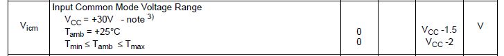
2. Build, and test the following circuit.note that a precise value for the 5k resistors is n't important. you can use 4.7k or 5.1k resistors.
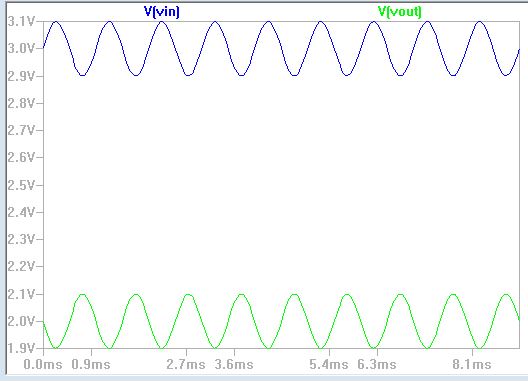
A. what is the common-mode voltage, VCM? Does VCM change? why or why not?
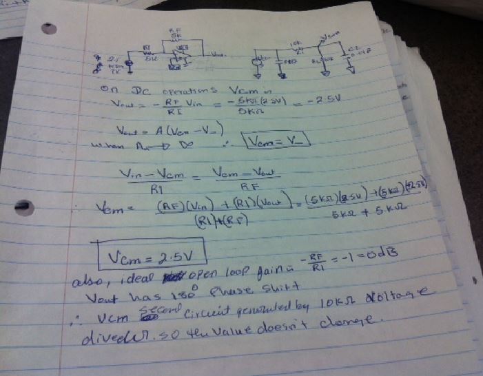
:- VCM is 2.5V. VCM does n't change because 10k voltage divider and op amp 1, however the following schematic is showing value does n't chage too.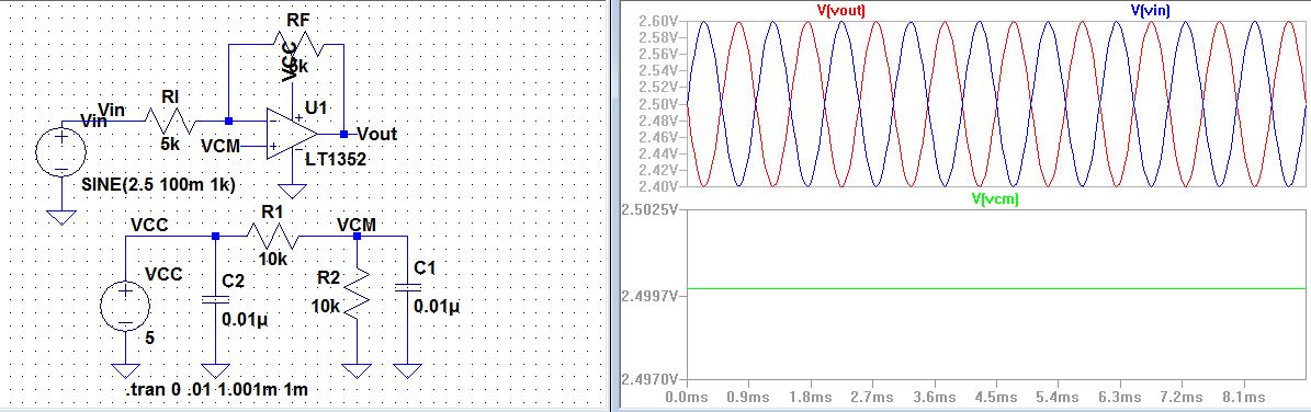
B. what is the ideal closed-loop gain?
:- closed loop-gain is A = (Vout/Vin) = (-R2/R1)
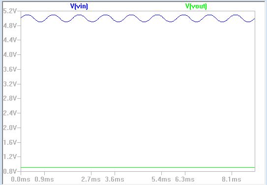
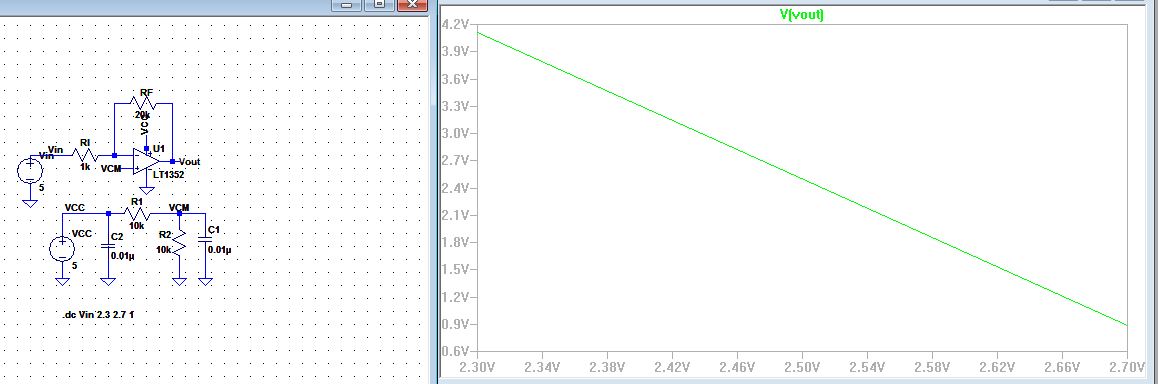
C. what is the ouput swing and what is it centered around?What happens if the input is n't centered around VCM, that is 2.5V? provide a detailed discussion illustrating that you understand what is going on.
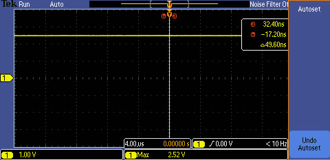
:- swing from 2.39V to 2.61V. Centered around is 2.5V. when the input voltage increasing, the output voltage is decreasing. the following schematic is showing what happening.
3. Explain how the following circuit can be used to measure the op-amp's offset voltage.
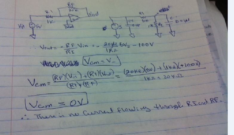
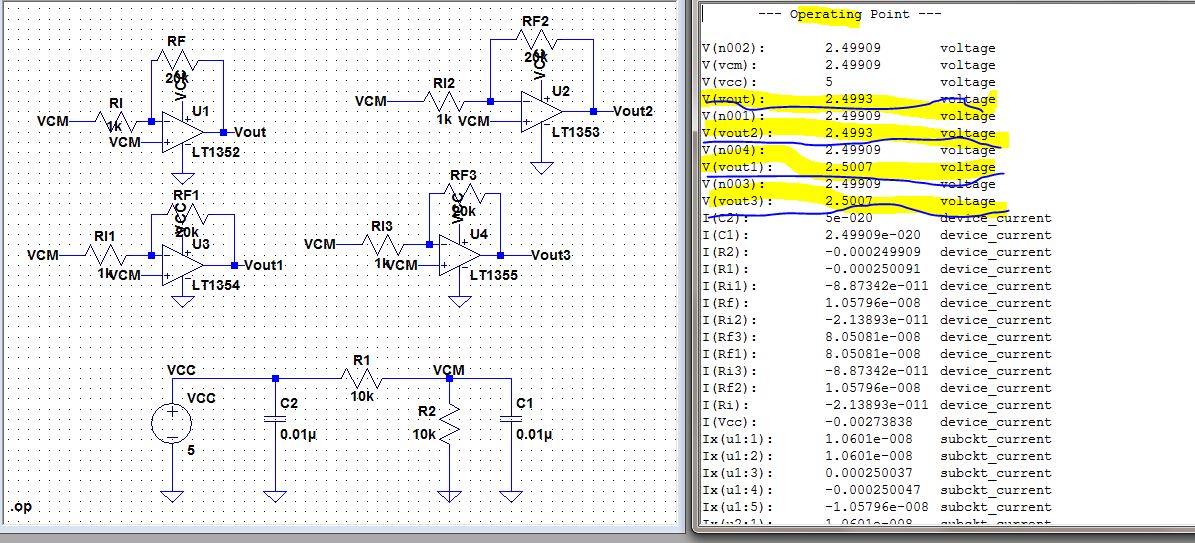
A. note that if the output voltage is precisely the same as VCM then the op-amp has no offset voltage (this is very possible). to measure small offset voltages increase the gain by increasing RF to 100k or larger. Explain what is hoing on.
:- there is no current flow throw R1 and RF because op-amps is ideal with zero offset. therefore, the following hand calculaton and schematic is shown.
:- the following schematic is shown that
Summary:-
Indeed, we learn how to operate ideal op-amp and real op-amp.
Add a return to the listing of your labs