Lab 3 - EE 420L
Authored
by: Roman Gabriele Ocampo
Email: ocampor5@unlv.nevada.edu
Date: February 24, 2014
Op-amps I
Prelab:
- Watch the op-amps I video available on the EE420L Lab 3 page
- Read the lab write-up provided on the lab website
Lab
Description and Goals:
The
goal of this lab to understand the function of an op-amp, as well as
recognize basic topologies and realize imperfections such as finite
gain and offset.
- Review the provided data sheet for the op-amp and answer the following questions:
- What are the max and min allowable common-mode voltages?
- What is a good estimate for the op-amp's open-loop gain?
- What is a good estimate for the offset voltage?
- Build and test the inverting amplifier circuit provided on the schematic on the lab 3 page.
- Answer the questions provided on the lab 3 page as it relates to the inverting amplifier circuit.
- Analyze the op amp schematic which is used to measure an op-amp's offset voltage.
Review of the LM324.pdf
The
maximum allowable common-mode voltage is Vcc - 1.5V. For our purposes,
Vcc is set to 5V, so the maximum and minimum common-mode voltage range
is -0.3V < Vcm < 3.5V.

From the diagram and datasheet entry below, a good estimation of the open-loop gain is 100dB or 100,000.


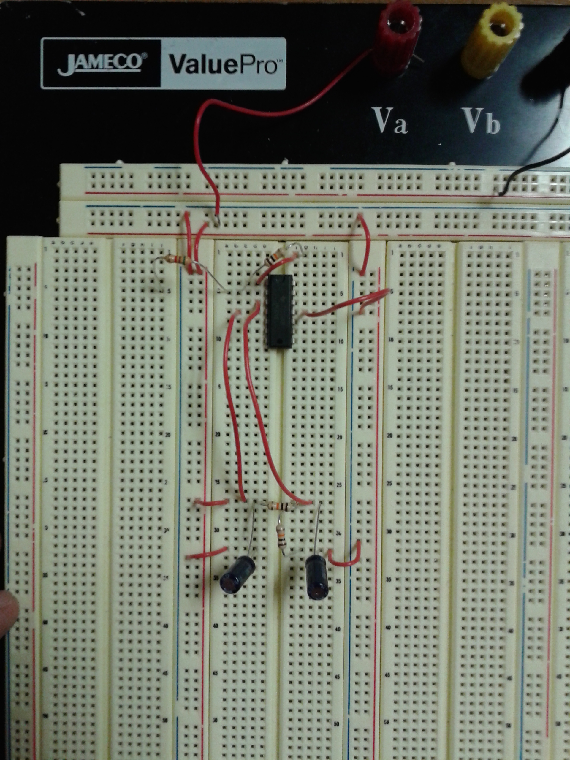
Inverting Amplifier Circuit
The schematic and a picture of the built circuit is found below:

VCM
is created through a voltage divider, therefore it is at a constant
2.5V. The ideal closed loop gain is given by -RF/RI = -1.
The
function generator that I had access to in the lab could not be set to
provide an AC signal smaller than 700mV, so the following waveforms
have been captured using an AC signal of 1V.

With
an AC input of 1V, the output swings between 1.5V and 3.5V, and it is
centered around 2.5V. The centering of Vout and Vin are inversely
related. No current flows into the op-amp, so the KCL equation at the
Vm node is (Vin-VCM)/RI = (VCM-Vout)/RF. RI and RF are equal, so an
increase in Vin causes a decrease in Vout, and vice versa.
The
maximum allowable input signal amplitude is 1V. This is because, as
illustrated above, the maximum VCM is 3.5V. So, for a Vin centered at
2.5V, an AC signal of 1V will cause VCM to hit its maximum. Any higher
than that, and the input MOSFETs of the amplifier will move into
triode, affecting the operation of the op-amp. If the gain of the
amplifier is increased to 10, the maximum input amplitude will drop to
0.1V.

The waveforms above are the result of a 1V signal through an amplifier with a gain of 10.
The
capacitors from VCC and VCM to ground are used to decouple the nodes,
causing them to be free from noise effects. The values on the
capacitors is not critical.
The input bias current is the
(average) current that flows out of both the non-inverting and
inverting inputs of the op-amp. For the op-amp used in this lab, the
input bias current is 20nA. In an ideal op-amp however, no current
flows into the input nodes. Therefore, input bias currents will cause
deviation from the ideal output voltage when large RI and RF
resistances are used, because the input bias current will load them.
The input offset current is the difference between the currents in the
two input terminals.
Measuring an Op-Amp's Offset Voltage

The
circuit above is used to measure the op-amp's offset voltage. Both
inputs are connected to VCM. Ideally, no current would flow through RI
and RF, so Vout would be equal to VCM. However, Vout will devate from
VCM if the op-amp amplifies its own input offset voltage. Therefore,
this circuit can be used to measure an op-amp's offset voltage by
taking the difference between Vout and VCM and dividing the difference
by the closed loop gain. Using this technique, and LTspice, the offset
voltage of 4 different op-amps can be calculated as part of the
experiment.

From
the above diagram, each op-amp's input offset voltage can be found by
taking the value of Vout, subtracting 2.5V, and then dividing by 200.
Return to the listing of my labs
Return
to the whole class reports
Return
to the EE420L site
Return to CMOSedu.com