Verilog-AMS
Tutorials using SMASH from CMOSedu.com (Return)
Tutorial 4 – Performing DC simulations
DC
analysis generally requires the change in sources over time. In SMASH to perform this you will have to
create your sources on the simulation level (i.e. the circuit file) instead of
the top level file (i.e. the .va file).
The reason for this is that the can SMASH IDE analyzes nodes through
different files but it does not analyze source names through files. A better way to think of it is that you can
sweep a source value but you cannot sweep a node value.
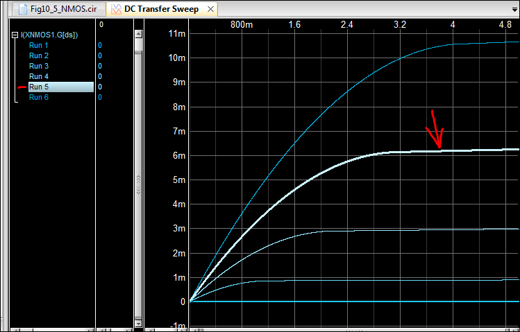
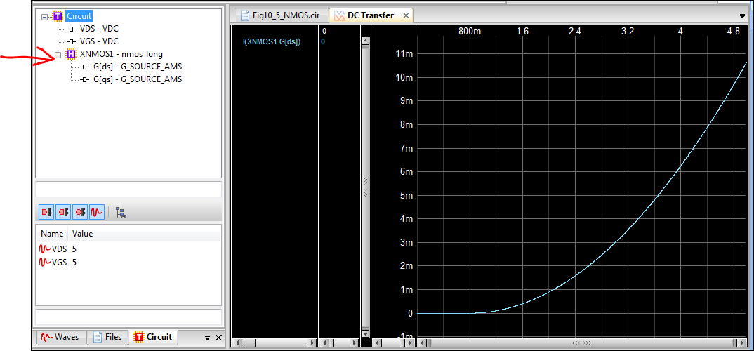
1. For this tutorial, we will simulate the IV
curve of an NMOS. If you refer to Figure
10.5, you will get the general idea of what our simulation will look like.
2. We will start the creation of the circuit
file the same as we have done in other tutorials. Once you have created your file you need to
add the voltage source and NMOS libraries (Vsource and NMOS).
3. For the next step you will build your
circuit instead of including a top level file (.elaborate command). These will resemble spice coding.
4. Recall that NMOS has three main points:
Drain, Source, and Ground. It will be at
these points where we will connect our voltage sources.
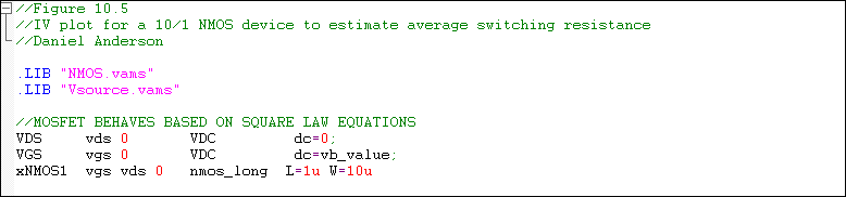
5. First let’s declare our voltage source that
will connect to the drain of our mosfet. The declaration format is as follows:
Source_Name, node1, node2, Verilog_module, parameter_values. For our first voltage source will look
something like the following: VDS vds 0 VDC dc=5;
This line of text created a voltage source named VDS connected to nodes
vds and 0(gnd), with this source be based off the VDC Verilog-AMS code module
(located in Vsource) and we passed a value of 5 to the dc parameter.
6. Now let’s create a second source named VGS
and follow the same syntax as before.
One thing we will change is that instead of passing 0 to the dc
parameter let’s pass “vb_value”. The
purpose of this variable will be explained later. This will look like:
VGS vgs 0 VDC dc=vb_value;
7. Now the final component will be our
NMOS. Naturally we would choose a name
like M1 for the mosfet name; however this will cause a problem. M1 is a very common mosfet reference and
because of this you cannot use it as a spice parameter and not a variable name
(the same thing will happen with other common names like R1 for resistor and D1
for diodes. Even if you do not get an
error it will see it as other types of components.) To prevent problems, we will use something more
specific like xNMOS1 instead.
8. If
you recall the names of the two voltage sources (VDS and VGS), you can see that
they represent the voltage from the drain-source and voltage from the
gate-source connections. This is where
we will share node names to simulate the connection in the circuit. Based on the follow syntax:
xNMOS1 vgs vds
0 nmos_long L=1u W=10u ;
we see
that we have our 2 voltage sources connected to the drain and gain of the
mosfet along with the source tied to ground (0). Also notice the parameters being passed are
the length and width of the mosfet.
NOTE:
the order of the models is always based on the Verilog-AMS modules. To verify proper connection make sure to
check the file to see that the orientation matches. For the NMOS, the order should be (gate,
drain, source). The order for the
voltage source is (positive, negative).
Keep this in mind when you wish to create negative sources. You can pass negative values or you can just
swap the orientation of the model when you “build it”
9. Verify your circuit is correct by saving
and reloading your circuit file. If no
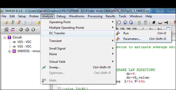
errors show up you are ready to perform a simulation. First let’s do a simple DC simulation on only
a single source. Select AnalysisàDC TransferàParameters. This will
open the parameter menu where you will select which source to sweep.
10. There are 3 basic parameters:
a. Parameter- this is used to select the type
of data that will be swept. It can be
temperature, voltage source, or current source
b. Device- based the parameter you are given a
list of found devices that can be swept.
It is important that the device are properly declared the will not
appear. For this tutorial you will not
see any current sources since we did not create any but you will see voltage
sources.
c. Value- this parameter holds the type of value that will be swept.
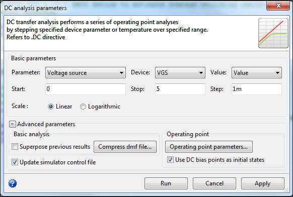
11. Below the basic parameters are the values
you need to enter. Start and Stop refer
to the starting and ending values for the sources. The STEP refers to the step size of the
simulation. The smaller the Step the
more accurate the simulation will be, but it will take longer to simulate.
12. After setting the parameters let’s simulate
the current across the mosfet (Drain to Source). Do this by selecting AnalysisàDC TransferàRun. A new window will
open asking you to add which signals to plot.
Expand the XNMOS1 (purple box) and select the G[ds] option. This will plot the current flowing through
those nodes (which is the current flowing from the drain to source.)
NOTE: If you do not have the circuit fully expanded
you need to close the window and do it manually. In the simulation window (black screen)
select ProbesàTrace
Signals and Nets after you have expanded the XMOS1 box. It should
now let you select the G[ds]. Then click add as you would for any
signal.
13. Now that we have seen a single source
sweep. Let’s sweep two sources so we can see the IV characteristics of the NMOS. First go back to the DC transfer
characteristics and change the source from VGS to VDS. Keep the settings the same (0 to 5 1m step)
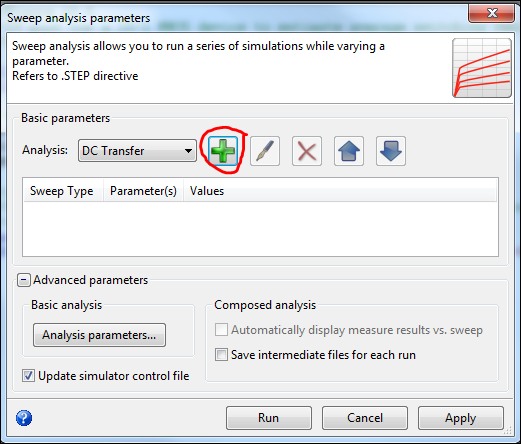
14. Next go to AnalysisàSweep.
A new window will open prompting for the analysis type. Select DC Transfer from the drop down
menu. The press the green plus (+)
symbol.
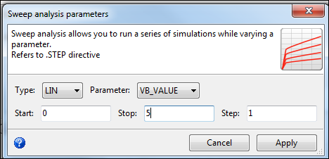
15. Another window will open up. In this window select LIN for type and choose the parameter VB_VALUE (this is the name of the parameter we passed to VGS when we declared it.) Then click Apply.
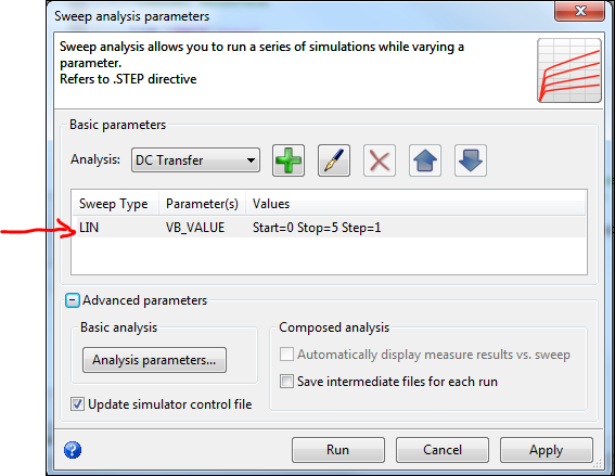
16. You will now be back at the sweep parameter screen but a new line of text will be visible. This is a confirmation on the type of sweep you will be performing. Click APPLY. Your main screen will now how simulations: a .DC LIN and a .STEP analysis. This will allow us to sweep two sources simultaneously. Select AnalysisàSweep then click on Run. You should not have to select which signal to plot since it should still be present since the last simulation.

17. When the simulation finishes you can select
each of the individual current lines to check there values.