Bad
Circuit
Design 12 - Using RC Networks and Miller Compensation
impedance node when trying to compensate an op-amp. In other words Miller compensation is, generally,
bad design. One may think, however, that by adding some RC networks here and there in an op-amp the
resulting additional poles and zeros can be placed so that Miller compensation can still be the better
design choice (that is, better than indirect compensation.) Using Miller compensation, even with the
addition of RC networks, is generally bad design.
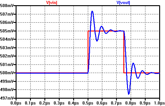
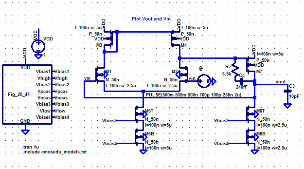
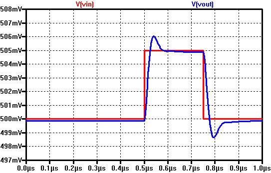
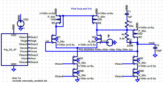
The step response of the op-amp seen in Fig. 24.8 with Rz = 1/gm = 6.5k and Cc reduced to 240 fF driving
a 10 pF load is seen below. This is a simple two-stage Miller compensated design with zero-nulling resistor
and it's bad design.
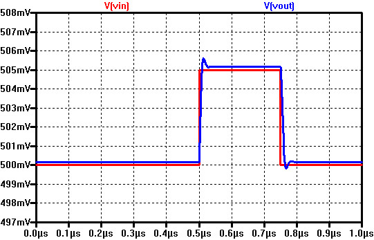
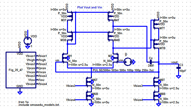
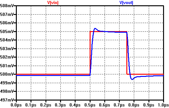
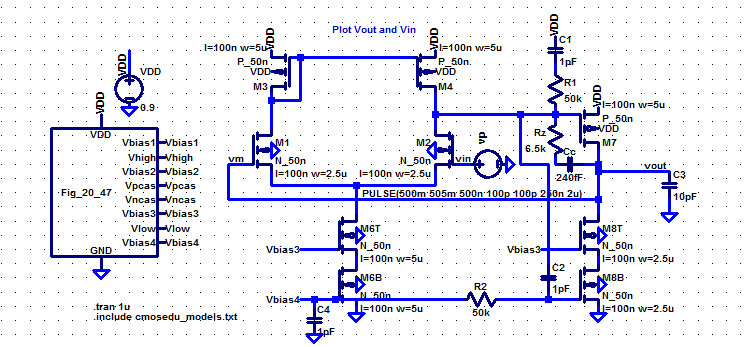
Below is the step response of the op-amp seen in Fig. 24.21 driving, again, a 10 pF load. This is a simple
two-stage indirect compensated design.
The layout size of each of these op-amps is roughly the same (the design above is slightly larger because
of Rz). The power consumption is precisely the same. Making the Rz track 1/gm over process, voltage, and
temperature (PVT) shifts is a practical concern as discussed in the book (see Fig. 24.15 and the associated
discussion). Clearly the design seen below (indirect compensation) using a split-length current mirror (SLCM)
load is more stable than the design above using Miller compensation and a zero nulling resistor.
For the same op-amp topology, e.g. a diff-amp followed by common-source amp, indirect compensated designs
can be 4 to 10 times faster and smaller than the equivalent Miller compensated design. A good estimate for
area is to look at the capacitor values in the op-amp. The stable design seen in Fig. 24.8 uses a 2.4 pF cap
while a 240 fF cap is used in the design in Fig. 24.21.
It's interesting to re-simulate this design without Rz and Cc. The result is actually more stable and slightly
faster than what is seen below (still slower than the design using indirect compensation). However, with no
load, or other load capacitances, the op-amp oscillates. This isn't robust or practical design.
indirect compensation.
Below we've added an AC path, via C2, from the output of the diff-amp to the gate of M8B to increase the
gain of the second stage. This will increase the effective capacitance on the output of the diff-amp helping to
stabilize the op-amp. Further, for pulses or higher frequencies, the output stage now behaves like a class AB
output (see Fig. 24.29, among other figures, for how to implement a true class AB output stage). A 50k resistor
and an additional 1 pF decoupling are added to isolate the DC voltage, Vbias4, from the AC signal coupled to
the gate of M8B. The layout size of this design is considerable larger than the indirect compensated design and
it's still slower.
There may be
situations where adding RC networks can be useful to improve the speed
of an op-amp; however,
it's bad design to add
these networks so that Miller compensation can be used instead of
indirect compensation.
For more information
Indirect
Feedback Compensation Techniques for Multi-Stage Operational Amplifiers or
the presentation here.
See also Vishal Saxena OpAmps Matlab Design
Kit.zip.