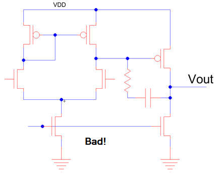
Bad Circuit
Design 3 - Compensating an Op-Amp
Perhaps
one of the biggest misses in 70s, 80s, and 90s in CMOS analog IC design
research was the
use
of split-length devices (first reported in the second edition of the CMOS
book in 2004) for
compensation.
These techniques have been developed and applied to 3 stage op-amp design where
there
are literally dozens of published papers that report less than quality designs,
especially
with
regard to biasing and topology. Here we won’t discuss three-stage designs or
using cascode
structures
(see how to connect the compensation capacitor in Fig. 24.29). For more information
about
three stage designs or design specifics for high-performance see Dr. Saxena’s
Master’s
Thesis:
Indirect
Feedback Compensation Techniques for Multi-Stage Operational Amplifiers or
the
presentation here.
See also Vishal Saxena OpAmps
Matlab Design Kit.zip.
Below
is a simple two-stage op-amp using Miller compensation with a zero-nulling resistor. This is
a
bad design. Using this approach the op-amp is slower, larger, and (for a fixed
speed requirement)
burns
more power.
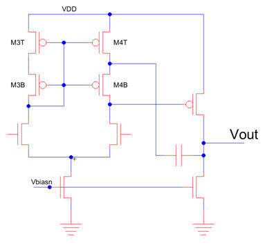
A
(much) better design uses split-length loads as seen below (Fig. 24.21). The
RHP zero is removed
and
the compensation capacitor can be 4 to 10 times smaller (so the op-amp is
faster!) Assuming
the
same widths for M3T/M3B and M4T/M4B they can be combined into a single MOSFET
with
the
lengths of the devices summed (see problem 6.14 on page 160). For DC biasing
purposes the
topology
above is exactly the same as the below topology.
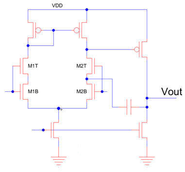
We
can apply the same technique to the diff-pair to get better power supply
rejection, see below.
This
topology, because the source of M2B isn’t at AC ground as is the source of M4T
above,
doesn’t
have as clean of settling as the split-length current mirror load above (the
zero is at a
lower
frequency than in the split-length loads) but the power supply rejection is
much better.
Again,
details are found in Dr. Saxena’s Thesis referenced
above.
In simple terms, never connect a
compensation capacitor back to a high-impedance node in a
multi-stage op-amp design, again see the presentation here.
Doing so is incredibly common but
it’s
bad design!
P.S.
Feeding the current through a compensation capacitor indirectly back to the
high-impedance
node
using a: 1) common-gate amplifier, 2) cascode structure, 3) current mirror, 4)
split-length
diff-pair
(SLDP), or 5) split-length current-mirror load (SLCL) is called indirect
compensation to
correctly
describe the circuit design technique. See pages 783 to 788 (see comment at the
bottom
of
page 788).
Sometimes,
when using one of these specific indirect paths, other names are used. For
example,
when
using a cascode structure the terminology “cascode compensation” may be used.
It’s best
(more
precise), however, to use a name that represents the more general compensation
technique
hence why “indirect compensation” is used in the book and (above) presentation.
No,
including the zero-nulling resistor, as seen in the
first figure above, doesn’t make connecting
the
compensation capacitor back to a high-impedance node okay. It’s still bad
design.