Bad Circuit
Design 11 - Using Split-Length Devices to replace a Cascode Structure
An example of split-length devices is seen in Fig. 24.21. In this
figure splitting the length is used to
provide an indirect (to the high-impedance output of the diff-pair)
current path for compensating the
op-amp.
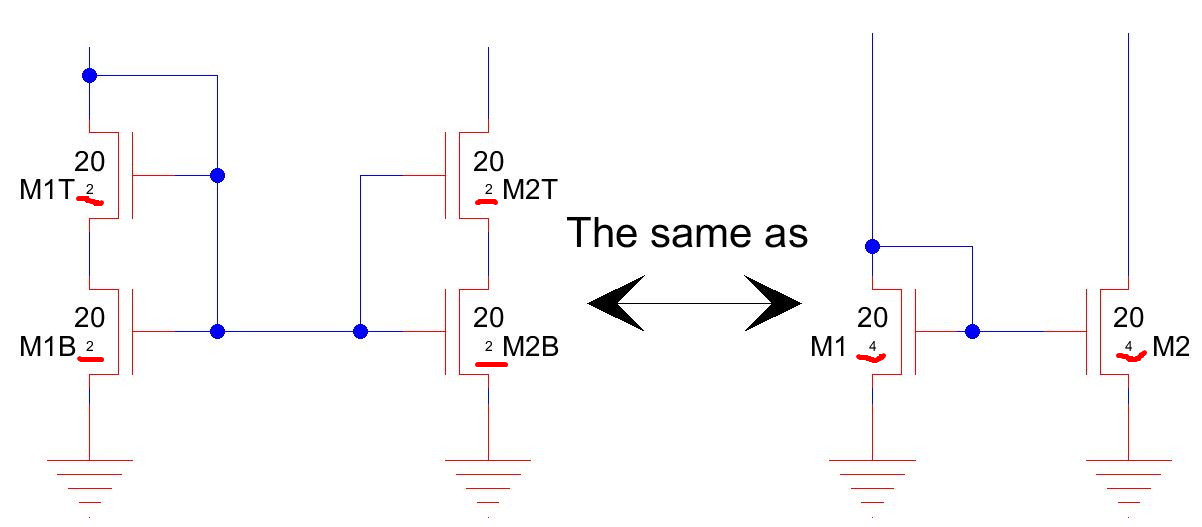
Seen below M1T and M1B, with W/Ls of 20/2, are equivalent to a
single MOSFET, M1, with a W/L
of 20/4. M2T and M2B are equivalent to M2. As discussed in the
book, problem 6.14 on page 160, M1B
and M2B can never operate in the saturation region.
The bad design comes when one tries to move M1B and M2B into the
saturation region by making M1T
and M2T both really wide (large W/L) so that each of their
gate-source voltages move towards VTHN
(overdrive voltage moves towards zero). Then, for example, VDSM1B = VGSM1B - VTHN. Of course we can
never really get M1B or M2B quite into the saturation region so
the split-length structure won't have
nearly as high of an output impedance as a cascode structure and thus
it can't replace it.
Here we indicate that replacing a cascode structure with a
split-length device is bad design,
not just because
of the lower output impedance, but also because the fT of the M1T and M2T devices
is inherently low.
We've driven their overdrive voltages towards zero. This, as
discussed in the book, introduces unwanted low
frequency parasitic poles and thus poor time-domain behavior (see here for additional
general comments).