Shadden Abdalla
November 30, 2018
EE421, Fall 2018
CMOS Switching Power Supply (SPS) Boost Converter
Contents
Summary of Results and
Tradeoffs…………………………………………………………….2-3
Result Tables and
Circuit Specifications……………………………………………………...4-10
Bandgap……………………………………………………………………………………...11-14
Comparator…………………………………………………………………………………...15-21
Buffer…………………………………………………………………………………………...22
Oscillator……………………………………………………………………………………23-24
NAND………………………………………………………………………………………….25
Inverters x8 and x64……………………………………………………………………………26
Ring oscillator and NAND…………………………………………...………………………28-31
Duty cycle and frequency.……………………………………………………………………28-29
NMOS Switch………………………………………………………………………………..31-33
Whole schematic
simulation with off-chip components…………………………………………34
Initial Conditions……………………………………………………...………………………....34
Choosing a Diode…………………………………………………….
…………………….……35
Load Resistance and
Current…………………………………………. ……………………..35-36
Capacitor and Ripple
Frequency and Tradeoffs…………………………………………………37
Input Current over
Voltage Divider……………………………………………………………...38
Choosing an Inductor and
Tradeoffs……………………………………………………………..39
Outputting 5V over
Varying VDD………………………………………………………………40
Circuit Reaction to
Varying Temperature……………………………………………………….41
On Chip Boost SPS
Schematic and Symbol…………………………………………………….42
Entire Layout…………………………………………………………………………………43-44
Bonding and Probe Pads…………………………………………………………………………45
Simulating Circuit with
Symbol and Off Chip Components…………………………………46-47
Efficiency Over VDDs of
3.75V and 4.75V…………………………………………………48-59
Efficiency vs. Load
Current……………………………………………………………...53 and 59
References*……………………………………………………………………………………...
60
*References were used for further
information. There were no works cited in this report.
---------------------------------------------------------------------------------------------------------------------
Summary
of Results and Tradeoffs
This report details the design, simulation and layout
of a CMOS Switching Power Supply (SPS) Boost Converter. This power supply reads
in an input voltage of VDD that could range from 3.75V to 4.75V and outputs a
constant output voltage of 5V. It consists of many components. The first is a
bandgap, which reads in the VDD input voltage and outputs a constant output
voltage of 1.25V. The second is a voltage divider that connects Vout to the comparator’s minus input, that draws between
10uA and 50uA of current: 36.78mA of current to be exact. The bandgap’s output
voltage is the positive input into the comparator. The comparator reads the two
input voltages and outputs a logic zero if the minus input is greater than the
positive input and outputs a logic one if the bandgap output voltage is greater
than the input voltage from the voltage divider. Then the output of the
comparator, enable, is sent into the oscillator and buffer that I made using a
NAND, thirty inverters, and then a buffer that sends a cleaned-up signal output
of the first ten inverters into the gate of the NMOS switch of size 48u/600n
with a multiplier of eight. More details about the outputs and project
specifications are below in the tables for easier viewing.
Choosing
NMOS Switch and Tradeoffs
The resistance of the MOSFET that I used is 31.25ohms
and the capacitance is 576fF. The NMOS has a larger width because it must be a
strong MOSFET that can switch quickly. Larger MOSFETs
with a larger width have very small internal gate resistances. The small
resistance causes it to be high-speed and be able to carry high currents. This
circuit generates resonance which will create a voltage that oscillates around
a point, which is what we see in our simulations as we try to reach 5 volts.
Because of the resonance and the oscillation that results from it, the MOSFET
holds a current that creates a voltage that oscillates. The drain to source
resistance is influenced by the gate to source voltage. Lowering the resistance
of the MOSFET causes the gate to source voltage to increase. Increasing the
temperature also causes the drain to source resistance to increase. The
capacitance is also extremely high in the MOSFET which is why we need the
buffer to reduce delay of capacitance. A tradeoff found when using a strong
NMOS is the larger layout versus less delay, however the layout can be reduced
by using fingers.
Choosing
Diode of 1N5819
I choose this diode because the
maximum voltage is 40V, average rectified forward current is 1A, dissipates
1.25W of power, maximum thermal resistance of 100 degrees Celsius per Watt.
This thermal resistance is perfect because I measured the operation of the
circuit up to 100 degrees Celsius. This diode is a
good choice for a power supply because it operates at temperatures up to 100
degrees Celsius and works at 90 degrees Celsius without any thermal runway.
Thermal runway is when the internal heat of the circuit increases much faster
than the circuit can dissipate that heat. When there is too much heat, the
circuit can fry and become destroyed. This diode is a good choice because it
operates at high temperatures and can handle a faster increase of heat up to 90
degrees Celsius, which is a high enough value for a power supply.
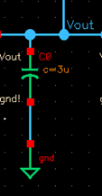
Choosing Capacitor and Tradeoffs
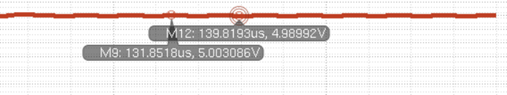
The output of my circuit oscillates around 5V with very little ripple because the capacitor I choose, 3u, is large enough to reduce ripple significantly. Capacitors are also affected heavily by temperature, and the amount of ripple current that the capacitor contains is related to temperature as well. When we fabricate this chip and put it on a printed circuit board, we will be using ceramic capacitors. The ceramic capacitors that we use that work at higher temperatures have less ripple current versus capacitors at lower temperatures. The capacitor works almost like a decoupling capacitor which is used to reduce noise especially in power supply signals. It is important to have a large capacitor when dealing with power signals because it helps smooth the signal and makes it easier to read. The ripple is reduced significantly, and the output voltage only oscillates from 4.98V to 5.003V. Since the frequency that I am using is above 10MHz, (it is 15MHz) this is considered a high-speed design. It is more difficult to increase the current when the speed is very high, so a LARGE CAPACITOR helps with that since at high speeds the impedance is lower because of the high frequency. The faster speed makes it harder to conduct large amounts of current because the impedance goes down which is one of the tradeoffs of using that frequency, however, adding a large capacitor gets rid of the issues and my circuit was able to conduct large amounts of current. Adding a large capacitor adds delay, however the buffer helps reduce that delay.
Choosing
Inductor and Tradeoffs
The frequency of my circuit is high which means that the impedance of the inductor will increase, and the capacitance of the capacitor will do the opposite. Because of the faster frequency, the impedance will rise which is a tradeoff, however, I wanted my design to be high speed. For there to be more current in the load resistor, the inductor value also must be lower because inductors will have higher impedances when there is a high frequency.
Thus, based on ohms law, we want to make the inductor smaller to get a higher current so that there is less impedance in the circuit.
 My
entire schematic including off chip components.
My
entire schematic including off chip components.
TABLES with Final Values
Output voltages at
varying VDD values
|
VDD |
VOUT (V) |
|
3.75V |
5.0005 |
|
4V |
5.00046 |
|
4.25V |
5.001628 |
|
4.5V |
5.02437 |
|
4.75V |
5.037032 |
Output voltages at
varying temperatures using VDD of 3.75V
|
Degrees Celsius |
VOUT (V) |
|
0 |
4.9887 |
|
25 |
5.0017 |
|
50 |
4.9931 |
Load and Voltage
Divider Current Values
|
Type of Current |
Value in mA |
|
Load
current RL |
20.008 |
|
Voltage
Divider current |
36.78 |
Off-chip
component values/names
|
Name |
Value |
|
Diode |
1N5819
OnSemi |
|
Load
resistor |
250ohms |
|
Capacitor |
3uF |
|
Resistor
used in voltage divider |
34kohms |
|
Inductor |
30uH |
Load Current for
Varying Temperatures, VDD = 3.75V
|
Temperatures
in Celsius |
Current
in mA |
|
0 |
19.955 |
|
25 |
20.001 |
|
50 |
19.937 |
|
75 |
19.907 |
|
100 |
19.8934 |
|
Average
Current |
19.93868 |
Load Current for
Varying Temperatures, VDD = 4.75V
|
Temperatures
in Celsius |
Current
in mA |
|
0 |
20.1347 |
|
25 |
20.1962 |
|
50 |
20.1326 |
|
75 |
19.949 |
|
100 |
20.0053 |
|
Average
Current |
20.08356 |
Inverters
used and values
|
Normal |
12u/6u |
|
Weak |
W=L=64
/ W=L=6u |
|
Normal
x8 |
48u/24u
with m=2 |
|
Normal
x64 |
48u/24u
with m=16 |
Frequency
and Duty Cycle
|
Frequency |
15.03MHz |
|
Duty
Cycle |
49% |
Efficiency Over Different Temperatures for a VDD of 3.75V
|
Temperatures in Celsius |
Efficiency (%) |
|
0 |
83 |
|
25 |
77 |
|
50 |
84.7 |
|
75 |
82.4 |
|
100 |
78.9 |
|
AVERAGE
EFFICIENCY |
81.2 |
Efficiency Over
Different Temperatures for a VDD of 4.75V
|
Temperatures in Celsius |
Efficiency (%) |
|
0 |
83 |
|
25 |
85.7 |
|
50 |
89 |
|
75 |
92.1 |
|
100 |
84.7 |
|
AVERAGE EFFICIENCY |
86.9 |
Efficiency Versus Load Current 3.75V
|
Temperature |
Load Current |
Efficiency |
|
0 |
19.955 |
83 |
|
25 |
20.001 |
77 |
|
50 |
19.937 |
84.7 |
|
75 |
19.907 |
82.4 |
|
100 |
19.8934 |
78.9 |
|
Average |
19.938 |
81.2 |
Efficiency Versus Load Current 4.75V
|
Temperature |
Load Current |
Efficiency |
|
0 |
20.13747 |
83 |
|
25 |
20.1962 |
85.7 |
|
50 |
20.1326 |
89 |
|
75 |
19.949 |
92.1 |
|
100 |
20.0053 |
84.7 |
|
Average |
20.0835 |
89.9 |
I(VDD) Values over
Varying Temperatures
|
Temperature in Celsius |
For VDD=3.75V |
For VDD=4.75V |
|
0 |
187.5mA |
263.89mA |
|
25 |
196.78mA |
158.56mA |
|
50 |
123.77mA |
151.42mA |
|
75 |
111.86mA |
144.23mA |
|
100 |
114.03mA |
141.77mA |
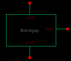
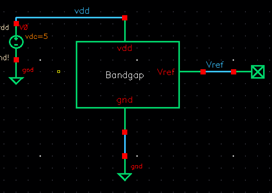
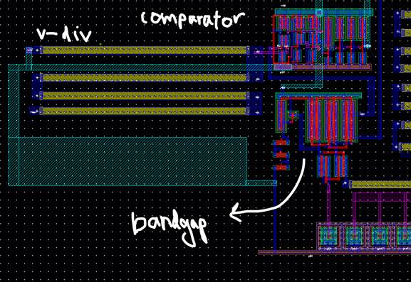
PART 1: BANDGAP
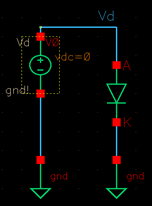
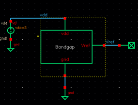
The bandgap circuit should read an input voltage and output a steady voltage of 1.25V.
Below is the schematic and symbol of the bandgap. 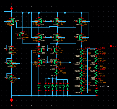
Bandgap simulations:
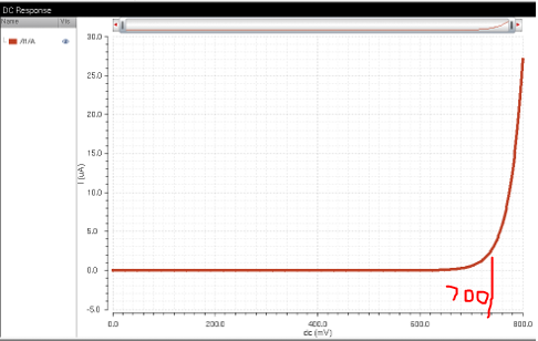
 The simulation
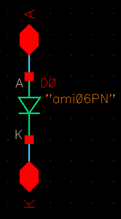
of the bandgap shows that it works as intended. It is tested with an input
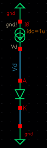
voltage of 5V and outputs a constant voltage of 1.25V. A parasitic PNP bipolar
transistor was also used in the bandgap circuit. The schematic, simulation and
layout of the PNP are below. The simulation shows the diode’s current which
increases at the switching point of a diode, about 0.7 volts or 700mV.
The simulation
of the bandgap shows that it works as intended. It is tested with an input
voltage of 5V and outputs a constant voltage of 1.25V. A parasitic PNP bipolar
transistor was also used in the bandgap circuit. The schematic, simulation and
layout of the PNP are below. The simulation shows the diode’s current which
increases at the switching point of a diode, about 0.7 volts or 700mV.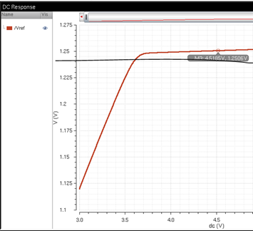
BANDGAP
TEMP
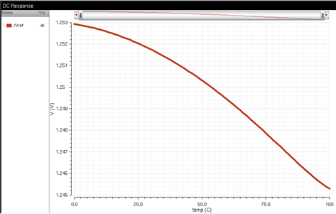
 Below is the
temperature simulation of the bandgap. The bandgap should output a constant
1.25V regardless of temperature. The graph plots the voltage change from a
temperature of 0 to 100 degrees Celsius. The voltage changes very slightly and
decreases from 1.253V to 1.245V which is a negligible change. The circuit also
works regarding temperature changes.
Below is the
temperature simulation of the bandgap. The bandgap should output a constant
1.25V regardless of temperature. The graph plots the voltage change from a
temperature of 0 to 100 degrees Celsius. The voltage changes very slightly and
decreases from 1.253V to 1.245V which is a negligible change. The circuit also
works regarding temperature changes.
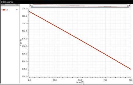
 To the right is
the temperature simulation of the PNP. The voltage changes very slightly with
the change in temperature. It decreases from 775mV to 550mV from 0 to 100
degrees Celsius.
To the right is
the temperature simulation of the PNP. The voltage changes very slightly with
the change in temperature. It decreases from 775mV to 550mV from 0 to 100
degrees Celsius.
 Then I laid out the bandgap. I used poly2 resistors to reduce layout size and to make the
design more concise.
Then I laid out the bandgap. I used poly2 resistors to reduce layout size and to make the
design more concise.
PART
2: COMPARATOR
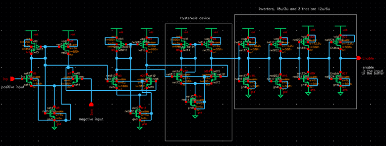 Below is the
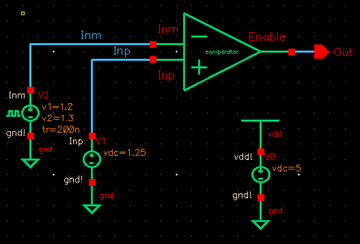
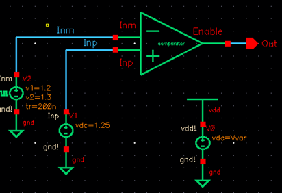
entire comparator and some zoomed in snips of the left, middle and right parts.
It consists of three differential amplifiers and four inverters. There are two
inputs, Inp and Inm, and an
output, Enable. Each differential amplifier introduces hysteresis so one of
them is labeled accordingly.
Below is the
entire comparator and some zoomed in snips of the left, middle and right parts.
It consists of three differential amplifiers and four inverters. There are two
inputs, Inp and Inm, and an
output, Enable. Each differential amplifier introduces hysteresis so one of
them is labeled accordingly.
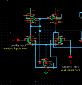 Left side: one differential amplifier and the inputs. I used four
terminal NMOS and PMOS devices of 6um/600nm widths and lengths respectively.
The bodies of all PMOS devices are tied to VDD. The bodies of all NMOS devices
are tied to gnd. The bandgap output of 1.25V should input to the Inp terminal and Vout after being
divided with a voltage divider should input into the Inm
terminal as highlighted in yellow.
Left side: one differential amplifier and the inputs. I used four
terminal NMOS and PMOS devices of 6um/600nm widths and lengths respectively.
The bodies of all PMOS devices are tied to VDD. The bodies of all NMOS devices
are tied to gnd. The bandgap output of 1.25V should input to the Inp terminal and Vout after being
divided with a voltage divider should input into the Inm
terminal as highlighted in yellow.
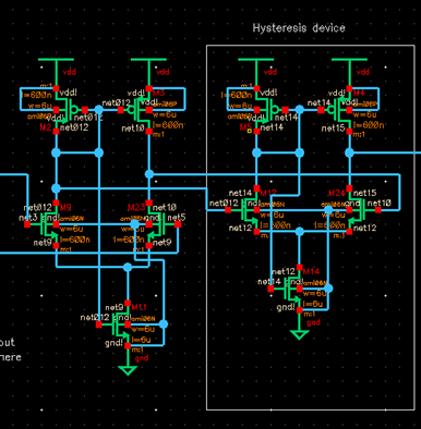 Middle: two differential amplifiers. I used four terminal NMOS
and PMOS devices of 6um/600nm widths and lengths respectively. The bodies of
all PMOS devices are tied to VDD and the bodies of all NMOS devices are tied to
gnd.
Middle: two differential amplifiers. I used four terminal NMOS
and PMOS devices of 6um/600nm widths and lengths respectively. The bodies of
all PMOS devices are tied to VDD and the bodies of all NMOS devices are tied to
gnd.
The right most PMOS and NMOS is connected to the first of
four inverters on the right side. The inverters sharpen the signal and since
there are four of them, they do not invert the signal. There would need to be
an odd number of inverters for the signal to be inverted because the even
number just cancels out the first inversions.
Right: inverters.
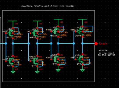 The first inverter has widths of 18um/3um which reduces the delay
in the output signal. When using an inverter of 18um/3um you can see in the
simulation below that the output changes exactly at the crossing point of both
the input signals. When all four of the inverters are of the same input,
however, the output is delayed slightly, and the input is not perfectly aligned
with the output. This is shown in the simulations below.
The first inverter has widths of 18um/3um which reduces the delay
in the output signal. When using an inverter of 18um/3um you can see in the
simulation below that the output changes exactly at the crossing point of both
the input signals. When all four of the inverters are of the same input,
however, the output is delayed slightly, and the input is not perfectly aligned
with the output. This is shown in the simulations below.
With four 12um/ 6um inverters on the left and with one 18um/3um inverter and three 12um/6um inverters on the right. It is apparent that the signal is slightly more accurate when using a 18um/3um inverter. The results are not extremely significant so technically you could use either topology.
 COMPARATOR
CIRCUIT SIMULATION – regular transient simulation
COMPARATOR
CIRCUIT SIMULATION – regular transient simulation
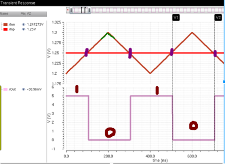 I simulated the
comparator to verify its accuracy before moving on. I mimicked the bandgap by
inputting a constant DC voltage of 1.25V into the positive input and inputted a
pulsing signal from 1.2V to 1.3V into the minus terminal because the output
from the voltage divider will not be a perfect signal; it will have ripples and
noise. A pulsing signal mimics the output from Vout
as closely as possible. I used a VDD of 5 volts for this smaller simulation
even though I will be using a range of 3.75V to 4.75V in my entire SPS
simulation. It is important to note that including a VDD of a different value
in a symbol and then using that symbol in the entire schematic will cause
significant error. The symbol must be saved without any VDD values so that it
can be controlled in the schematic where the symbol is used. As stated in the
previous project requirements, when the input from the minus terminal is
greater than 1.25V from the bandgap the output goes low and when the input from
the minus terminal is lower than 1.25V the output goes high.
I simulated the
comparator to verify its accuracy before moving on. I mimicked the bandgap by
inputting a constant DC voltage of 1.25V into the positive input and inputted a
pulsing signal from 1.2V to 1.3V into the minus terminal because the output
from the voltage divider will not be a perfect signal; it will have ripples and
noise. A pulsing signal mimics the output from Vout
as closely as possible. I used a VDD of 5 volts for this smaller simulation
even though I will be using a range of 3.75V to 4.75V in my entire SPS
simulation. It is important to note that including a VDD of a different value
in a symbol and then using that symbol in the entire schematic will cause
significant error. The symbol must be saved without any VDD values so that it
can be controlled in the schematic where the symbol is used. As stated in the
previous project requirements, when the input from the minus terminal is
greater than 1.25V from the bandgap the output goes low and when the input from
the minus terminal is lower than 1.25V the output goes high.
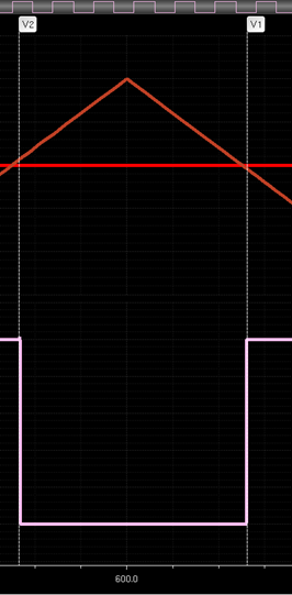
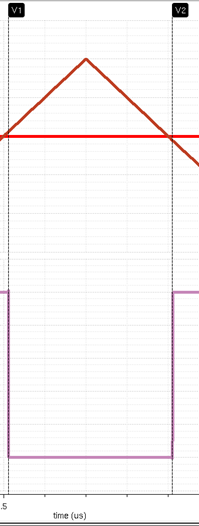
This is demonstrated in
the simulation to the left. The area highlighted shows the input from the minus
terminal as high, showing a 0 logic output.
Just directly to its left you can see the bandgap voltage rising higher than the input voltage from the pulsing signal that mimics the Vout voltage, and the output voltage that corresponds to that relationship is a logic 1. After the simulations were complete, I laid out the comparator schematic. The pins are vdd!, gnd!, Inp, Inm and Enable. Inm is the input from the voltage divider, Inp is the input from the bandgap, and Enable is the output that feeds into the buffer before reaching the switch.
PARAMETRIC TEMPERATURE
SIMULATION - COMPARATORS
Parametric:
 I simulated
comparator’s functionality in regard to changing
temperature using a parametric analysis from 0 to 100 degrees Celsius. I kept
the step size small, 5 degrees Celsius to see if there is any variation of the
simulation in regard to specific temperatures. There
was no significant variation.
I simulated
comparator’s functionality in regard to changing
temperature using a parametric analysis from 0 to 100 degrees Celsius. I kept
the step size small, 5 degrees Celsius to see if there is any variation of the
simulation in regard to specific temperatures. There
was no significant variation.
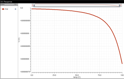 DC sweep: The voltage only went down to 4.99V from 5V as the
temperature increased from 0 degrees Celsius to 100 degrees Celsius.
DC sweep: The voltage only went down to 4.99V from 5V as the
temperature increased from 0 degrees Celsius to 100 degrees Celsius.
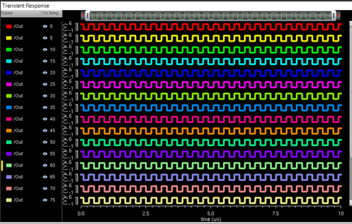
PARAMETRIC SIM OF VARYING VOLTAGE
 When I first ran this simulation, I used a VDD of 5V. To make sure
that the simulation works in my entire circuit with a VDD of 3.75V-4.75V, I
implemented a variable over my VDD and ran a parametric simulation to test all of those voltages. I choose 5 voltages in that range.
When I first ran this simulation, I used a VDD of 5V. To make sure
that the simulation works in my entire circuit with a VDD of 3.75V-4.75V, I
implemented a variable over my VDD and ran a parametric simulation to test all of those voltages. I choose 5 voltages in that range.
The comparator’s output
is the same for every voltage tested using the parametric analysis. This shows
that the comparator will work with the VDD in the entire circuit when
simulating it altogether.
---------------------------------------------------------------------------------------------------------------------
PART 3: BUFFER
 The buffer
consists of many parts. The first part is the oscillator that will create the
oscillating signal that results from the comparator. The oscillator’s input
will be the output of a NAND. Then two of the outputs of the first ten
inverters are fed into another NAND whose output is fed into three more
inverters to sharpen the signal. The first inverter that takes in the signal
from the NAND is a normal 12um/6um inverter. The second one is the same normal
inverter multiplied by eight and the third one is the normal inverter
multiplied by sixty-four. The output of the largest inverter is the signal that
reaches the switch (NMOS). The larger the inverter, the sharper the output is.
From the buffer, we can calculate the frequency and the duty cycle
of our signal.
The buffer
consists of many parts. The first part is the oscillator that will create the
oscillating signal that results from the comparator. The oscillator’s input
will be the output of a NAND. Then two of the outputs of the first ten
inverters are fed into another NAND whose output is fed into three more
inverters to sharpen the signal. The first inverter that takes in the signal
from the NAND is a normal 12um/6um inverter. The second one is the same normal
inverter multiplied by eight and the third one is the normal inverter
multiplied by sixty-four. The output of the largest inverter is the signal that
reaches the switch (NMOS). The larger the inverter, the sharper the output is.
From the buffer, we can calculate the frequency and the duty cycle
of our signal.
First, I simulated the oscillator to make sure that it worked. The oscillator I used consists of thirty-one inverters. The first ten are normal sized, 12um/6um, the next ten are weak inverters with lengths and widths of 6um on each device, and the last eleven are regular inverters.
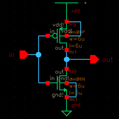
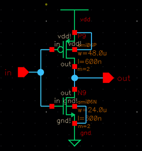
 Below is the
normal inverter’s schematic, layout and symbol.
Below is the
normal inverter’s schematic, layout and symbol.
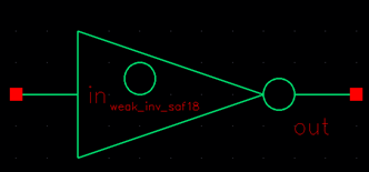
 Then I created a
weak inverter, with length and width of 6um for both devices. Below is the
schematic, layout and symbol. I put a circle inside of the weak inverter’s
symbol so that it is easier to differentiate from the other inverters.
Then I created a
weak inverter, with length and width of 6um for both devices. Below is the
schematic, layout and symbol. I put a circle inside of the weak inverter’s
symbol so that it is easier to differentiate from the other inverters.
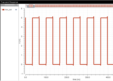
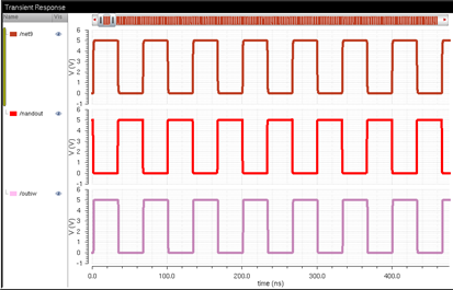
ENTIRE OSCILLATOR
Then, I tested the oscillator with thirty-one inverters to make sure it oscillates before connecting it to the other components. It oscillates so now we can connect it to the other components and test it. I decided to use a NAND as my inverter to simplify the circuit. NANDS are commonly used when creating buffers, which is what we are doing in this case. Two NANDs connected to each other act like a buffer. Since I am using a NAND as an inverter, I am going to reduce the number of inverters I have in my oscillator in order to continue to have an odd number of inverters.
Entire oscillator simulation below:
I created a separate schematic and layout for a ring
oscillator with only thirty inverters, specific for connecting the entire
circuit. I did not simulate this circuit because it is not supposed to work.
This buffer will not oscillate because it has an even number of inverters.
 Below is the
oscillator with an even number of inverters.
Below is the
oscillator with an even number of inverters.
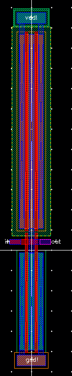
Below is the layout of
the inverter.
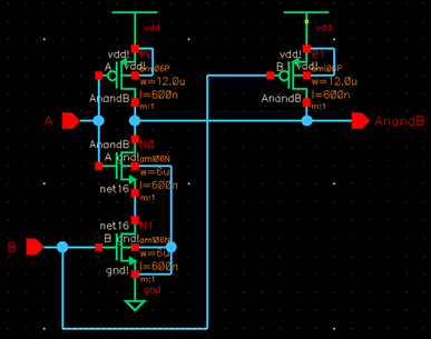
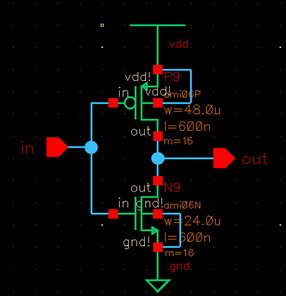
NAND
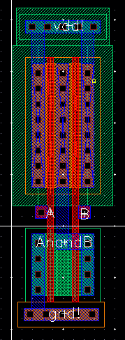 I created a
NAND using four terminal MOSFETs, PMOSes of
12um/0.6nm and NMOSes of 6um/0.6um.
I created a
NAND using four terminal MOSFETs, PMOSes of
12um/0.6nm and NMOSes of 6um/0.6um.
NORMAL
INVERTER x8
 To simplify the
layout, I first calculated the width that would result from multiplying the
original dimensions by eight.
To simplify the
layout, I first calculated the width that would result from multiplying the
original dimensions by eight.
12 um * 8 = 96 um
6 um * 8= 48 um
Instead of creating an inverter with these widths, I divided the goal width by two and instead increased the multiplier of my inverter by two to make the layout more concise.
 layout of the x8 inverter
Normal inverter multiplied by 8 symbol
NORMAL
INVERTER x64
12 um * 6;4 = 768 um
6 um * 64 = 384 um
Instead of using these values, I used 48 um and 24 um with a multiplier of 16 to simplify the layout and make it as concise as possible. If one were to layout an inverter of the entire size without multipliers, the height of the inverter would be the entire height of a chip, and would cause immense error, cost too much and take up too much room in the entire layout of the chip. Our goal is to make the layout as small as possible, and multipliers help achieve that goal.
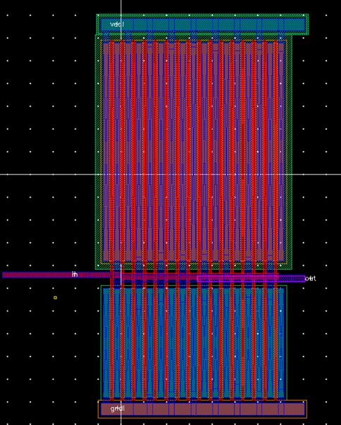 Below is the
layout of the inverterx64 with multipliers of 16.
Below is the
layout of the inverterx64 with multipliers of 16.
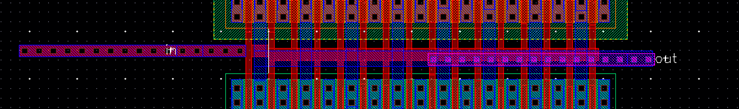
The contacts are zoomed in for better viewing. The input is connected to metal1-poly connectors and the output is connected to metal1 to metal 2 vias.
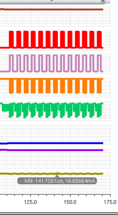
Now we have all of the parts and
we can put them all together to find the duty cycle, frequency, and the output
that be the input to the switch (NMOS) that will drive the current that we
need.
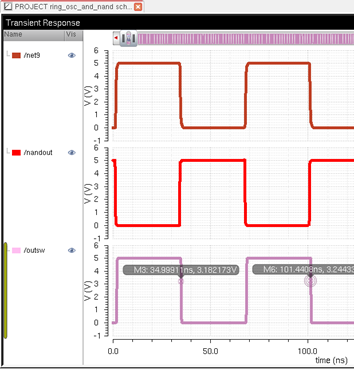
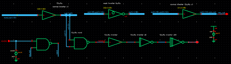 RING OSCILLATOR WITH NAND
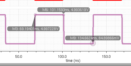
T = period = 101.44ns-34.99ns = 66.5ns
F = 1/T= 1/ 66.5nanoseconds=
15.03MHz
frequency
 DUTY
CYCLE
DUTY
CYCLE
Duty cycle is how much
more time it is high than it is low. It is high for 31.96 nanoseconds and it is
low for 33.5nanoseconds. So the duty cycle is 31.96 /
(31.96 + 33.5) = 0.488 so there is a 49% duty cycle.
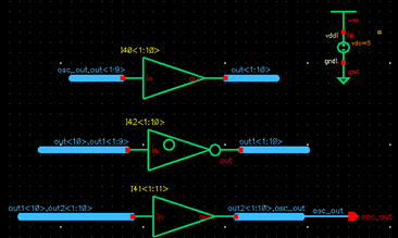
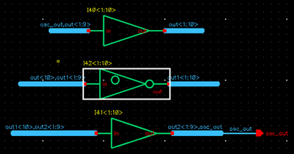
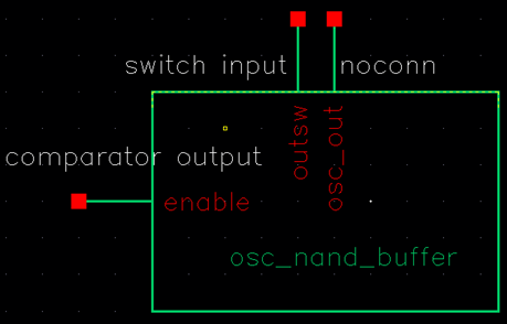
The symbol for
the NAND input, the oscillator and the buffer is
below:
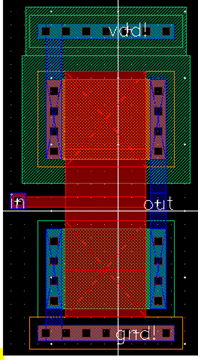
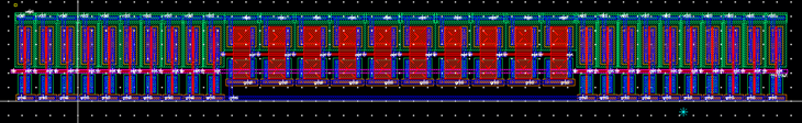
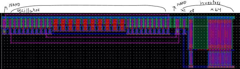 LAYOUT for the entire NAND input,
oscillator and the buffer:
LAYOUT for the entire NAND input,
oscillator and the buffer:
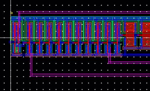
The
photo on the left shows the input NAND and the first ten normal inverters and
the first two weak inverters.
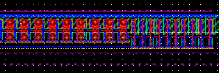
The
photo below shows the center, the rest of the weak inverters and all ten of the
final normal inverters.
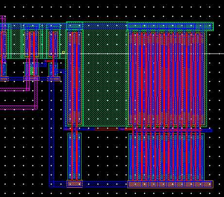
To
the left are the final NAND which leads to the normal inverter, inverterx8 and
inverterx64.
---------------------------------------------------------------------------------------------------------------
 PART 4: NMOS
SWITCH
PART 4: NMOS
SWITCH
The NMOS switch needs to be a strong MOSFET that can switch
quickly. Larger MOSFETs with a larger width have very small internal gate
resistances. The small resistance causes it to be high-speed and be able to
carry high currents. This circuit generates resonance which will create a
voltage that oscillates around a point, which is what we see in our simulations
as we try to reach 5 volts. Because of the resonance and the oscillation that
results from it, the MOSFET holds a current that creates a voltage that
oscillates. The drain to source resistance is influenced by the gate to source
voltage. Lowering the resistance of the MOSFET causes the gate to source
voltage to increase. Increasing the temperature also causes the drain to source
resistance to increase. The capacitance is also extremely high in the MOSFET
which is why we need the buffer to reduce the delay from the capacitance.
Resistance of the MOSFET:
The MOSFETs we used are in the C5
process in which the RN’ value of an NMOS is 20kohms. We can calculate the
entire resistance by using the equation:
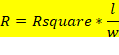
In this case, Rsquare is 20kohms, l= 600nm and w=48u*8=384um. The width
is multiplied by 8 because I am using a multiplier of 8. Increasing the width
decreases the resistance because of the relationship between the l and w in the
equation, since w is in the denominator.
![]()
This resistance is
extremely small and is almost negligible.
Capacitance of the MOSFET:
In the C5 process, the C’ox is 2.5fF/um^2. To calculate the CoxN
we can use the equation:
![]()
![]()
![]() = 576fF which is higher than
we would want ideally. Since this
capacitance is larger, we can see that the capacitance goes up and the
resistance goes down. This is one of the tradeoffs of a larger switch.
= 576fF which is higher than
we would want ideally. Since this
capacitance is larger, we can see that the capacitance goes up and the
resistance goes down. This is one of the tradeoffs of a larger switch.
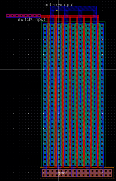 LAYOUT
OF THE SWITCH
LAYOUT
OF THE SWITCH
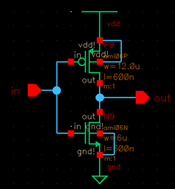
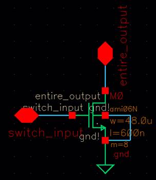
I
used an NMOS with multiplier of 8 to simplify my layout and make it more
concise. The source of the NMOS device is connected to ground and the gate is
connected to some metal one to poly connectors. The output from the oscillator
and buffer should be the input to the gate, which is labeled switch_input. The drain of the NMOS is where the output of
the circuit, which should be 5V, will be read.
-------------------------------------------------------------------------------------------------------------------
ENTIRE SCHEMATIC with off chip components
Below I will discuss how I simulated the entire schematic
with off chip components and why I choose these specific sizes and
specifications.
Initial
conditions:
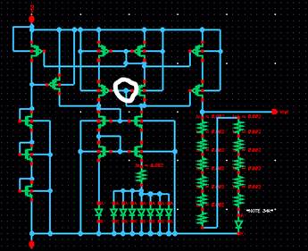 For
the schematic to simulate, there had to be some initial conditions set in the
circuits. There were two initial conditions that I simulated. The first one is the input to the switch and
the second one is a net in the bandgap that needed an initial condition to
begin.
For
the schematic to simulate, there had to be some initial conditions set in the
circuits. There were two initial conditions that I simulated. The first one is the input to the switch and
the second one is a net in the bandgap that needed an initial condition to
begin.
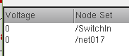
 Diode
Diode
 Diode model
text file: on Semiconductor Schottky Diode 1N5819. I chose this diode because
maximum voltage is 40V, average rectified forward current is 1A, and non-repetitive
peak current is 25A. It dissipates 1.25W of power and has a maximum thermal
resistance of 100 degrees Celsius per Watt which is good characteristic for
measuring the circuit’s outputs over varying temperatures that include 100
degrees Celsius. The maximum thermal resistance is 45 degrees Celsius per Watt.
This diode is a good choice for a power supply because it operates at
temperatures up to 100 degrees Celsius and works at 90 degrees Celsius without
any thermal runway. Thermal runway is when the internal heat of the circuit
increases much faster than the circuit can dissipate that heat. When there is
too much heat, the circuit can fry and become destroyed. This diode is a good
choice because it operates at high temperatures and can handle a faster
increase of heat up to 90 degrees Celsius, which is a high enough value for a
power supply.
Diode model
text file: on Semiconductor Schottky Diode 1N5819. I chose this diode because
maximum voltage is 40V, average rectified forward current is 1A, and non-repetitive
peak current is 25A. It dissipates 1.25W of power and has a maximum thermal
resistance of 100 degrees Celsius per Watt which is good characteristic for
measuring the circuit’s outputs over varying temperatures that include 100
degrees Celsius. The maximum thermal resistance is 45 degrees Celsius per Watt.
This diode is a good choice for a power supply because it operates at
temperatures up to 100 degrees Celsius and works at 90 degrees Celsius without
any thermal runway. Thermal runway is when the internal heat of the circuit
increases much faster than the circuit can dissipate that heat. When there is
too much heat, the circuit can fry and become destroyed. This diode is a good
choice because it operates at high temperatures and can handle a faster
increase of heat up to 90 degrees Celsius, which is a high enough value for a
power supply.
Above is the
model file that I put in the project folder.
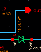
 Load Resistor and load current
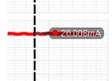 The load current shown
in yellow is 19.5mA which shows that the circuit can drive currents near 20mA.
Decreasing the load resistor can increase the current even further.
The load current shown
in yellow is 19.5mA which shows that the circuit can drive currents near 20mA.
Decreasing the load resistor can increase the current even further.
![]() è
è ![]()
 Increasing the Load Resistor
decreases the load current. This is because of how ohms law works. If Vout = 5V and RL=300ohms, I = 5V/300ohms which is 16.6mA.
I increased the load current to 300 ohms to demonstrate, which is shown
on the left. The current reduced by about 3mA.
Increasing the Load Resistor
decreases the load current. This is because of how ohms law works. If Vout = 5V and RL=300ohms, I = 5V/300ohms which is 16.6mA.
I increased the load current to 300 ohms to demonstrate, which is shown
on the left. The current reduced by about 3mA.
To the right is the load
current with changing temperatures.
 Capacitor
and Ripple and Frequency Tradeoffs
Capacitor
and Ripple and Frequency Tradeoffs
 The output of the circuit
oscillates around 5 volts. This is possible with less ripple because the
capacitor is large enough to reduce the ripple significantly. Capacitors are
also affected heavily by temperature, and the amount of ripple current that the
capacitor contains is related to temperature as well. When we fabricate this
chip and put it on a printed circuit board, we will be using ceramic
capacitors. The ceramic capacitors that we use that work at higher temperatures
have less ripple current versus capacitors at lower temperatures. The capacitor
works almost like a decoupling capacitor which is used to reduce noise
especially in power supply signals. It is important to have a large capacitor
when dealing with power signals because it helps smooth the signal and makes it
easier to read. The ripple is reduced significantly, and the output voltage
only oscillates from 4.98V to 5.003V. Since the frequency that I am using is
above 10MHz, (it is 15MHz) this is considered a high-speed design. It is more
difficult to increase the current when the speed is very high, so a LARGE
CAPACITOR helps with that since at high speeds the impedance is lower because
of the high frequency. The faster speed makes it harder to conduct large
amounts of current because the impedance goes down which is one of the
tradeoffs of using that frequency, however, adding a large capacitor gets rid
of the issues and my circuit was able to conduct large amounts of current.
The output of the circuit
oscillates around 5 volts. This is possible with less ripple because the
capacitor is large enough to reduce the ripple significantly. Capacitors are
also affected heavily by temperature, and the amount of ripple current that the
capacitor contains is related to temperature as well. When we fabricate this
chip and put it on a printed circuit board, we will be using ceramic
capacitors. The ceramic capacitors that we use that work at higher temperatures
have less ripple current versus capacitors at lower temperatures. The capacitor
works almost like a decoupling capacitor which is used to reduce noise
especially in power supply signals. It is important to have a large capacitor
when dealing with power signals because it helps smooth the signal and makes it
easier to read. The ripple is reduced significantly, and the output voltage
only oscillates from 4.98V to 5.003V. Since the frequency that I am using is
above 10MHz, (it is 15MHz) this is considered a high-speed design. It is more
difficult to increase the current when the speed is very high, so a LARGE
CAPACITOR helps with that since at high speeds the impedance is lower because
of the high frequency. The faster speed makes it harder to conduct large
amounts of current because the impedance goes down which is one of the
tradeoffs of using that frequency, however, adding a large capacitor gets rid
of the issues and my circuit was able to conduct large amounts of current.
 Input
current Over Voltage Divider
Input
current Over Voltage Divider
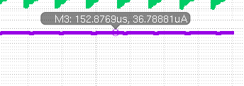
The input current over the voltage dividers is about 36.8uA which is within the range that I was aiming for which is in between 10uA and 50uA. The input supplies a high enough current.
To achieve this, I used 34k resistors to create a 3:1 voltage divider and supply 1.25 volts. I used these resistors to attain a current within the 10uA to 50uA range using Ohms law, V=IR.
 V=IR
V=IR
5V = I * (34k + 34k + 34k + 34k)ohms
5V = I * (136k ohms)
I = 5V / 136,000ohms = 36.76uA which is almost the same as the current in the simulation.
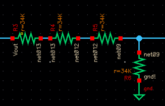
VOLTAGE DIVIDER
The 3:1 voltage divider divides the 5V output voltage into 1.25V (the input to the minus terminal of the comparator) to match the voltage of the bandgap circuit.
To prove this: Vin * R2/(R2+R1) = Vout ⇒ 5V * (34kohms / 136kohms)
= 5V * (0.25)[no unit here because
the kohms cancel each other to form a ratio, creating
the voltage divider] = 1.25V.
Choosing an Inductor &
Current Tradeoffs
![]() The frequency of my circuit is
high which means that the impedance of the inductor will increase, and the
capacitance of the capacitor will do the opposite. Because of the faster
frequency, the impedance will rise which is a tradeoff, however, I wanted my design
to be high speed. For there to be more current in the load resistor, the
inductor value also must be lower because inductors will have higher impedances
when there is a high frequency.
The frequency of my circuit is
high which means that the impedance of the inductor will increase, and the
capacitance of the capacitor will do the opposite. Because of the faster
frequency, the impedance will rise which is a tradeoff, however, I wanted my design
to be high speed. For there to be more current in the load resistor, the
inductor value also must be lower because inductors will have higher impedances
when there is a high frequency.
Thus, based on ohms law, we want
to make the inductor smaller to get a higher current so that there is less
impedance in the circuit.
These equations help us select
what inductor to choose:
Delta iL
is calculated to be 5% of the maximum average current which is estimated to be 5%
of 20mA and is 0.001A.
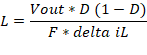
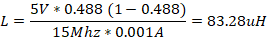
This value is a rough estimate,
and when testing my circuit, I choose a much smaller inductor value of 30uA for
the current to increase.
When simulating the inductor
value of 30uA, the current across the inductor is 76.27mA.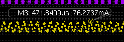
Recalculating the value using
this amperage:
0.00381A = 5%
![]()
---------------------------------------------------------------------------------------------------------------------
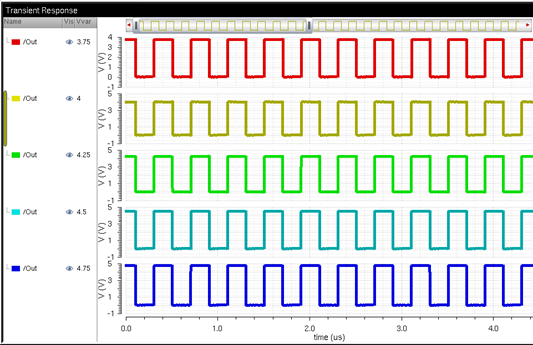
PART 5: Output of 5V over a varying voltage input
of 3.75V to 4.75V
![]() I used a parametric analysis with a step size of 5 to measure the output
over varying voltages of 3.75V to 4.75V to make sure that my simulation works
for every value in the range I was given. All five of the input values worked.
I used a parametric analysis with a step size of 5 to measure the output
over varying voltages of 3.75V to 4.75V to make sure that my simulation works
for every value in the range I was given. All five of the input values worked.
![]() Testing
the circuit’s reactions to varying temperatures from 0 to 50 degrees Celsius
Testing
the circuit’s reactions to varying temperatures from 0 to 50 degrees Celsius
![]()
![]() I used parametric analysis to simulate
the output voltage Vout, regarding varying
temperatures from 0 to 50 degrees Celsius. The simulation above shows that all
three voltages are about 5V exactly, and the circuit works in with varying
temperatures. The diode I choose helps with that since it operates well in
relationship to higher temperatures.
I used parametric analysis to simulate
the output voltage Vout, regarding varying
temperatures from 0 to 50 degrees Celsius. The simulation above shows that all
three voltages are about 5V exactly, and the circuit works in with varying
temperatures. The diode I choose helps with that since it operates well in
relationship to higher temperatures.
ON
CHIP BOOST SPS SCHEMATIC
![]() This
schematic is made into a symbol which will be on the chip and is tested
separately with the off-chip components.
This
schematic is made into a symbol which will be on the chip and is tested
separately with the off-chip components.
![]()
To
the left is the symbol view of the schematic above which will be used for the
simulations with the on-chip components.
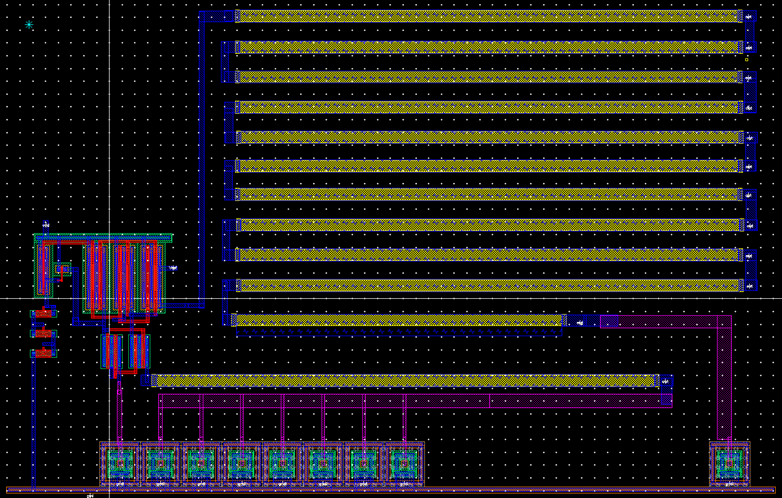
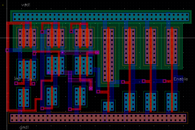
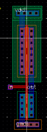
LAYOUT
![]()
Layout
of the on-chip components
![]()
![]()
![]()
BONDING
AND PROBE PADS
The
output feeds into the Vfeed back so we would only
need one probe pad. The photo below is extremely exaggerated as if the pad on
the die is larger than the components on the PCB. Ideally there would be a
trace connecting the components to the package and that would be wire bonded to
the pad on the die.
![]()
![]()
![]()
![]()
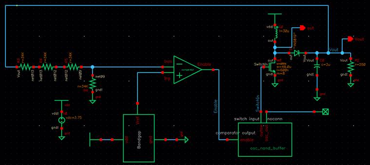
![]() Circuit with symbol
Circuit with symbol
![]()
![]()
![]()
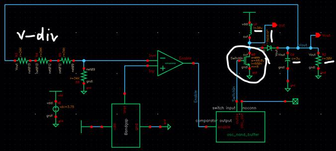
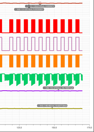
The
above simulation shows the output voltage at 5V, the load current at 20mA and
the current over the voltage divider at 36.8mA which is in between 10mA and
50mA. The signal, enable, that is the output of the comparator and then enters
the buffer to output the signal, switchin, which is
what enables and disables the switch and allows the whole circuit to work
properly as shown above.
Simulation starts at 100u
and ends at 300u to reduce unnecessary viewing of the startup signal.
EFFICIENCY
for 4.75v
![]()
For this efficiency calculation, I will be using 2 VDD
values of 3.75V and 4.75V. I will
also only simulate from about 215us to 300us because that is when the signal is
at steady state. This reduces error when calculating the average current
because of the startup current and voltages.
The
schematic below shows Vout, the load current and the
current of our battery with changing temperatures from 0 to 100 degrees
Celsius.
![]() The blue
traces are the load current, the green traces are the currents over VDD and
the red is the output voltage.
The blue
traces are the load current, the green traces are the currents over VDD and
the red is the output voltage.
![]()
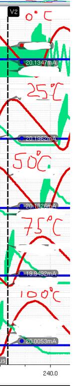
![]() The left is the load current with
varying temperature, the middle is Vout with varying temperature, and the left
is I(VDD) with varying temperature. The current goes down with rising
temperature.
The left is the load current with
varying temperature, the middle is Vout with varying temperature, and the left
is I(VDD) with varying temperature. The current goes down with rising
temperature.
![]()
Load
Current for Varying Temperatures, VDD = 4.75V
|
Temperatures
in Celsius |
Current
in mA |
|
0 |
20.1347 |
|
25 |
20.1962 |
|
50 |
20.1326 |
|
75 |
19.949 |
|
100 |
20.0053 |
|
Average Current |
20.08356 |
Now using the I(VDD) values found over varying temperatures, I
calculated the efficiency of the circuit.
![]()
SIMULATING
EFFICIENCY FOR 4.75V
For 0 degrees Celsius using RMS:
Rms(I(VDD))
= 112.9mA
![]()
![]()
For 0 degrees Celsius
using Average:
![]() Average(I(VDD))
= 25.3mA
Average(I(VDD))
= 25.3mA ![]()
For 25 degrees Celsius
using Average:![]()
![]()
![]() For 50 degrees Celsius
using Average:
For 50 degrees Celsius
using Average:
![]()
![]() For 75 degrees Celsius
using Average:
For 75 degrees Celsius
using Average:
![]()
![]() For 100 degrees Celsius
using Average:
For 100 degrees Celsius
using Average:
![]()
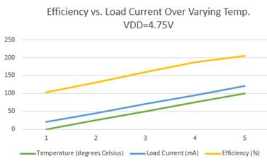
Based on these results, the
efficiency was best using 75 degrees Celsius.
Efficiency Over Different Temperatures for a VDD of 4.75V
|
Temperatures in Celsius |
Efficiency (%) |
|
0 |
83 |
|
25 |
85.7 |
|
50 |
89 |
|
75 |
92.1 |
|
100 |
84.7 |
|
AVERAGE
EFFICIENCY |
86.9 |
![]()
Based
on this graph comparing efficiency and the load current over varying
temperatures over a VDD of 4.75, it is apparent that as the temperature
increases, the load current also increases as well as the efficiency. They are
all correlated.
SIMULATING EFFICIENCY
FOR 3.75V
![]() I
used another parametric analysis to simulate the changes in voltages, the load
current and the current over vdd.
I
used another parametric analysis to simulate the changes in voltages, the load
current and the current over vdd.
![]()
To the left is the simulation with
markers for I(VDD) for VDD=3.75V. The straight lines across are the load
current values, and the cleaner oscillations are the output voltages, Vout which oscillate from 4.99V to 5.002V.
![]()
![]() The
left image shows the load current values over varying temperatures. The right
image shows the I(VDD) values for VDD= 3.75.
The
left image shows the load current values over varying temperatures. The right
image shows the I(VDD) values for VDD= 3.75.
Load
Current for Varying Temperatures, VDD = 3.75V
|
Temperatures
in Celsius |
Current
in mA |
|
0 |
19.955 |
|
25 |
20.001 |
|
50 |
19.937 |
|
75 |
19.907 |
|
100 |
19.8934 |
|
Average Current |
19.93868 |
Calculating
efficiency using the average I(VDD)
![]()
For a temperature of 0
degrees Celsius:
Average
current is: 32:11mA
![]()
![]()
For a temperature of 25
degrees Celsius:
![]() Average
current is:
Average
current is:
![]()
For a temperature of 50
degrees Celsius:
Average
current is:![]()
![]()
For a temperature of 75
degrees Celsius:
Average
current is:
![]()
![]()
For a temperature of 100
degrees Celsius:
![]() Average
current is:
Average
current is:
![]()
Efficiency Over Different Temperatures for a VDD of 3.75V
|
Temperatures in Celsius |
Efficiency (%) |
|
0 |
83 |
|
25 |
77 |
|
50 |
84.7 |
|
75 |
82.4 |
|
100 |
78.9 |
|
AVERAGE
EFFICIENCY |
81.2 |
![]() Based
on this graph comparing efficiency and the load current over varying
temperatures over a VDD of 3.75, it is apparent that as the temperature
increases, the load current also increases as well as the efficiency. They are
all correlated.
Based
on this graph comparing efficiency and the load current over varying
temperatures over a VDD of 3.75, it is apparent that as the temperature
increases, the load current also increases as well as the efficiency. They are
all correlated.
References
Baker,
R. Jacob. CMOS: Circuit Design, Layout,
and Simulation. IEEE Press, 2010.
Glaser,
Chris. “Does Inductor Ripple-Current Percentage Still Matter in Low-Power
Step-Down Converters?” Electronic Design,
23 Nov. 2015, www.electronicdesign.com/power/does-inductor-ripple-current-percentage-still-matter-low-power-step-down-converters.
Hauke,
Brigitte. “Basic Calculation of a Boost Converter's Power Stage - Texas
Instruments.” Texas Instruments - Basic
Calculation of a Boost Converter's Power Stage, Jan. 2014,
www.ti.com/lit/an/slva372c/slva372c.pdf.
Joshi,
Anoop. “Http://Ljournal.ru/Wp-Content/Uploads/2017/03/a-2017-023.Pdf.” Testing PSRR with High-Frequency Ripple -
Cadence, 2017, doi:10.18411/a-2017-023.
Li,
Jasper. “How to Select a Proper Inductor for Loaw
Power Boost Converter - Texas Instruments.” Texas
Instruments- How to Select a Proper Inductor for Low Power Boost Converter,
June 2016, www.ti.com/lit/an/slva797/slva797.pdf.
Zednicek,
Tomas. “Ripple Current and Its Effects on the Performance of Capacitors.” European Passive Components Institute,
30 Aug. 2017,
passive-components.eu/ripple-current-and-its-effects-on-the-performance-of-capacitors/.