TIA and VFTD Test Chip
Gonzalo Arteaga (arteag1@unlv.nevada.edu)
R. Jacob Baker (rjacobbaker@gmail.com)
Tyler Ferreira (ferret1@unlv.nevada.edu)
James
Mellott (
Eric Monahan (
Angsuman Roy (angsumanroy@gmail.com)
This
test chip was fabricated using the AMS 0.35um SiGe
(S35) process and consists of the following circuitry:
·
256
Stage VFTD with 4 Paths (Very Fast Transient Digitizer)
·
4
TIA test Structures (with and without APD input)
Pad Frame/Key
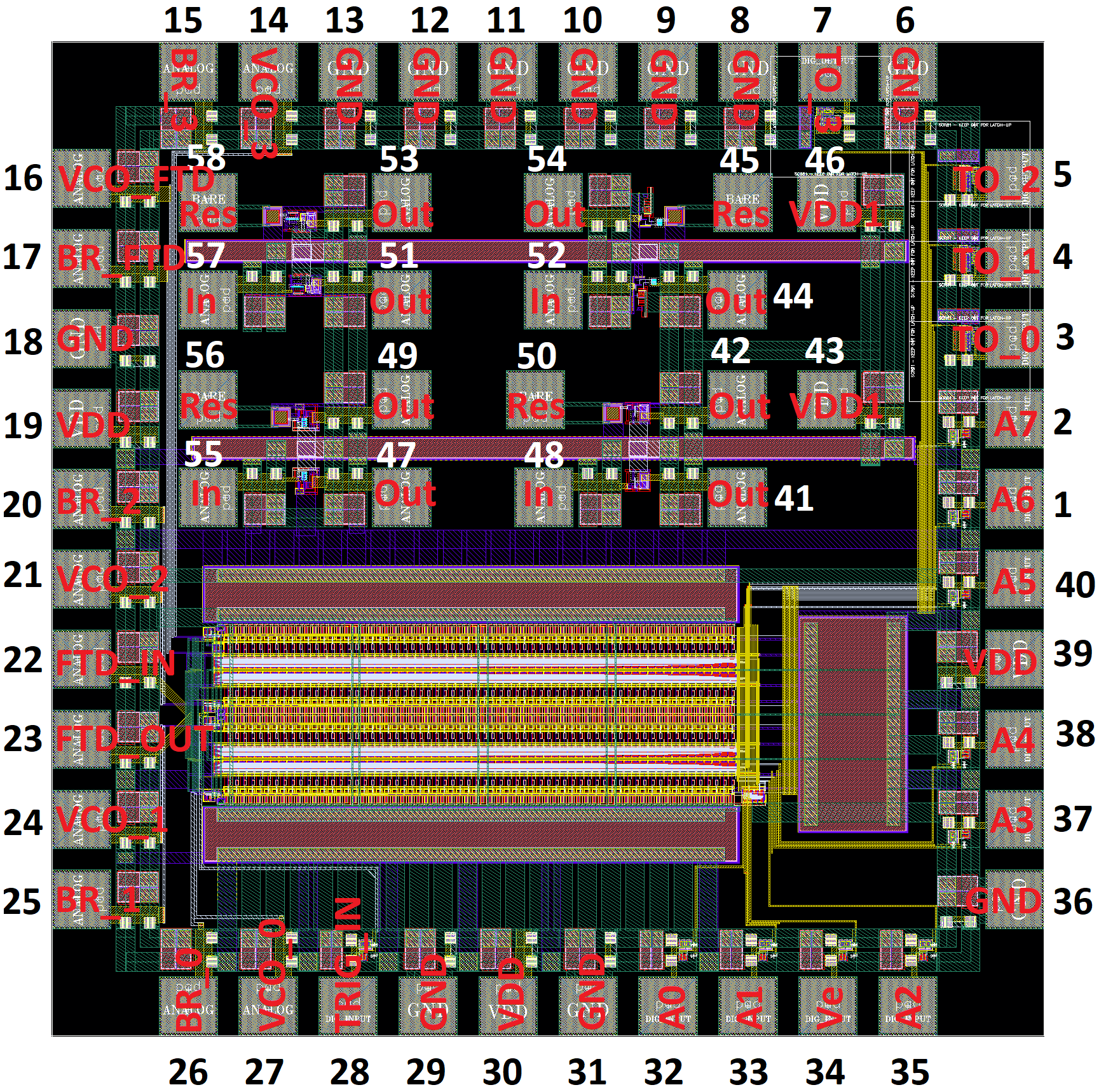
Pin Table
|
Pin # |
Name on Pad
Key |
Pin
Description |
|
1 |
A6 |
Decoder 6
input |
|
2 |
A7 |
Decoder 7 input |
|
3 |
TO_0 |
Trigger out for path 0 |
|
4 |
TO_1 |
Trigger out
for path 1 |
|
5 |
TO_2 |
Trigger out for path 2 |
|
6 |
GND |
Ground
connection for all on chip devices |
|
7 |
TO_3 |
Trigger out
for path 3 |
|
8 |
GND |
Ground
connection for all on chip devices |
|
9 |
GND |
Ground
connection for all on chip devices |
|
10 |
GND |
Ground
connection for all on chip devices |
|
11 |
GND |
Ground
connection for all on chip devices |
|
12 |
GND |
Ground
connection for all on chip devices |
|
13 |
GND |
Ground
connection for all on chip devices |
|
14 |
VCO_3 |
Control
voltage for path 3’s time delay |
|
15 |
BR_3 |
Bias
resistor for VCO for path 3 |
|
16 |
VCO_FTD |
Control
voltage for 256 stages’ time delay |
|
17 |
BR_FTD |
Bias
resistor for VCO for FTD stages |
|
18 |
GND |
Ground
connection for all on chip devices |
|
19 |
VDD |
VDD
Connection for VFTD |
|
20 |
BR_2 |
Bias
resistor for VCO for path 2 |
|
21 |
VCO_2 |
Control
voltage for path 2’s time delay |
|
22 |
FTD_In |
Analog input
for VFTD |
|
23 |
FTD_Out |
Analog
output for VFTD |
|
24 |
VCO_1 |
Control
voltage for path 1’s time delay |
|
25 |
BR_1 |
Bias
resistor for VCO for path 1 |
|
26 |
BR_0 |
Bias
resistor for VCO for path 0 |
|
27 |
VCO_0 |
Control
voltage for path 0’s time delay |
|
28 |
Trig_In |
Trigger
input for VFTD |
|
29 |
GND |
Ground
connection for all on chip devices |
|
30 |
VDD |
VDD
Connection for VFTD |
|
31 |
GND |
Ground
connection for all on chip devices |
|
32 |
A0 |
Decoder 0
input |
|
33 |
A1 |
Decoder 1 input |
|
34 |
Ve |
Enable voltage input for
decoder |
|
35 |
A2 |
Decoder 2 input |
|
36 |
GND |
Ground connection for
all on chip devices |
|
37 |
A3 |
Decoder 3 input |
|
38 |
A4 |
Decoder 4 input |
|
39 |
VDD |
VDD Connection for VFTD |
|
40 |
A5 |
Decoder 5 input |
|
41 |
Out |
Output for NSTEC TIA 1
without APD input |
|
42 |
Out |
Output for NSTEC TIA 1
with APD input |
|
43 |
VDD1 |
VDD connection for TIA test
structures |
|
44 |
Out |
Output for common source
TIA without APD input |
|
45 |
Res |
Resistor pad for APD for
common source TIA |
|
46 |
VDD1 |
VDD connection for TIA
test structures |
|
47 |
Out |
Output for Atollo TIA without APD input |
|
48 |
In |
Analog Input for NSTEC
TIA 1 |
|
49 |
Out |
Output for Atollo TIA with APD input |
|
50 |
Res |
Resistor pad for APD for
NSTEC TIA 1 |
|
51 |
Out |
Output for NSTEC TIA 2
without APD input |
|
52 |
In |
Analog input for common
source TIA |
|
53 |
Out |
Output for NSTEC TIA 2
with APD input |
|
54 |
Out |
Output for common source
TIA with APD input |
|
55 |
In |
Analog input for Atollo TIA |
|
56 |
Res |
Resistor pad for APD for
Atollo TIA |
|
57 |
In |
Analog input for NSTEC
TIA 2 |
|
58 |
Res |
Resistor pad for APD for
NSTEC TIA2 |
VDD and Ground Pins
(VFTD VDD pins 19, 30, 39 TIA VDD pins 43, 46 Global GND pins 6,
8-13, 18, 29, 31, 36)
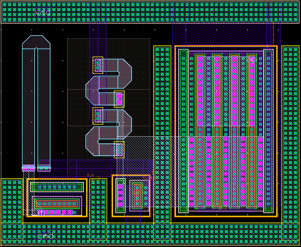
Figure 1: NSTEC TIA 1
NSTEC TIA 2
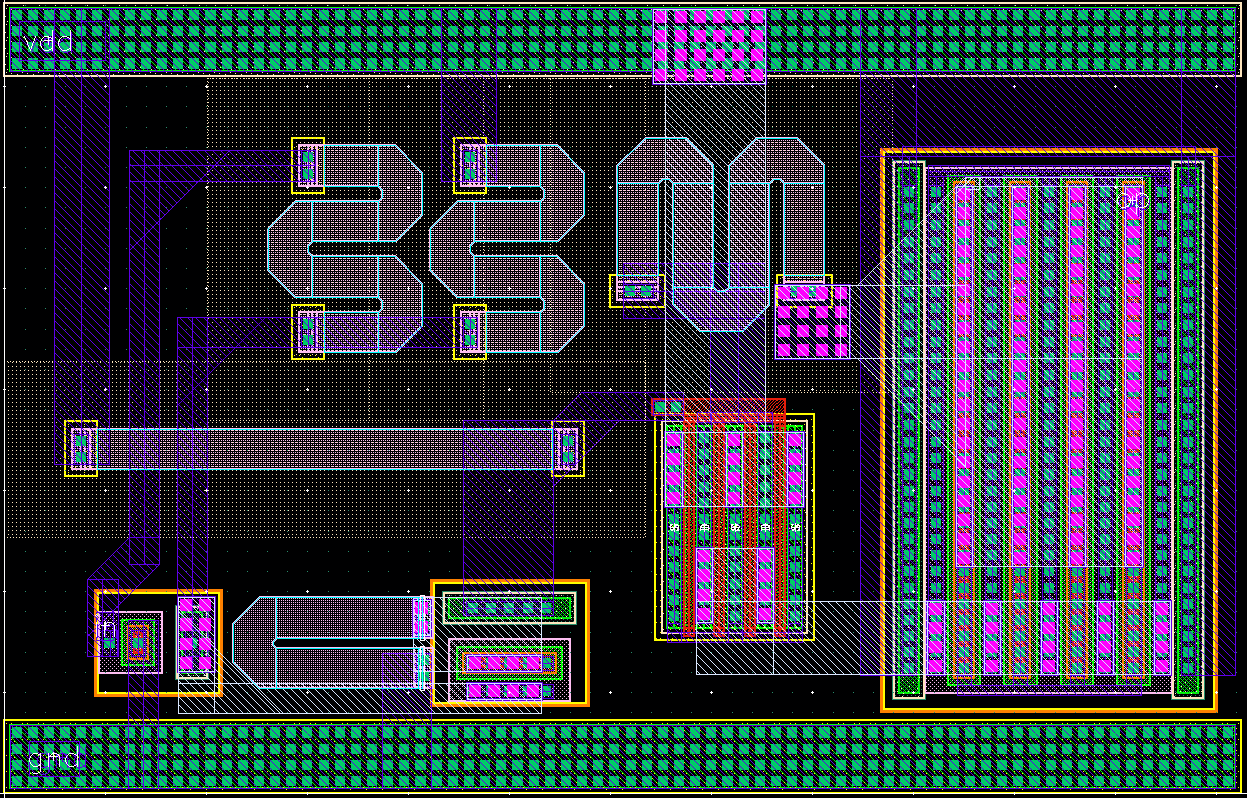
Figure 2: NSTEC TIA 2
Atollo TIA 1
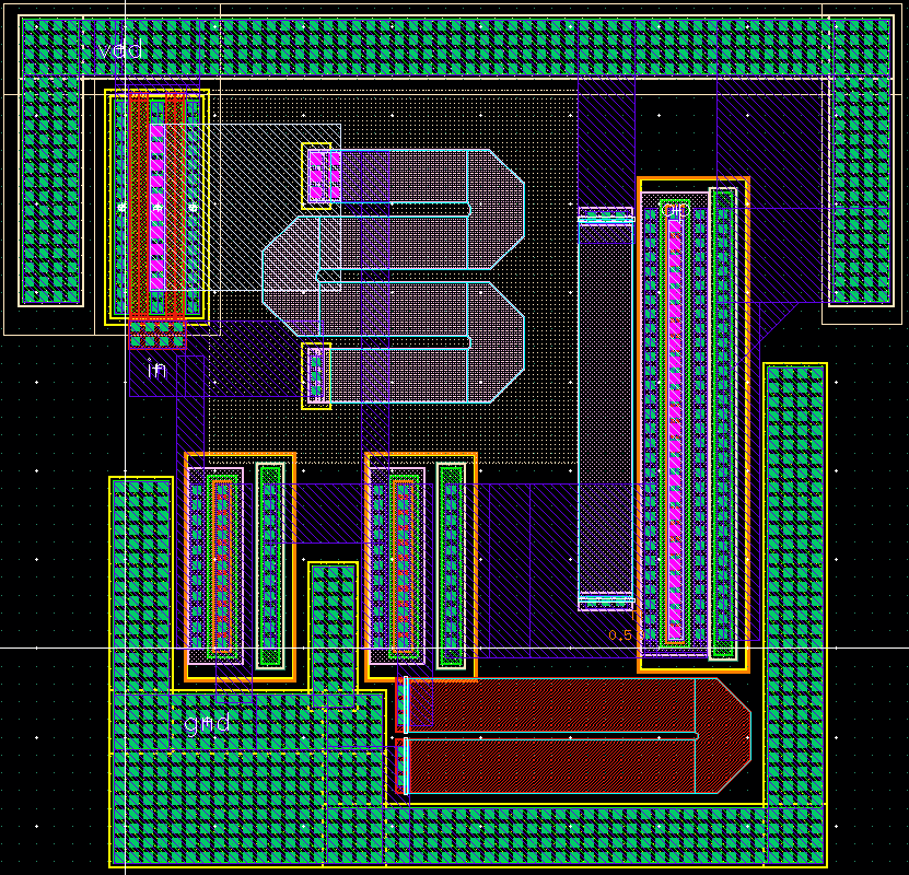
Figure 3: ATOLLO TIA 1
Common Source TIA
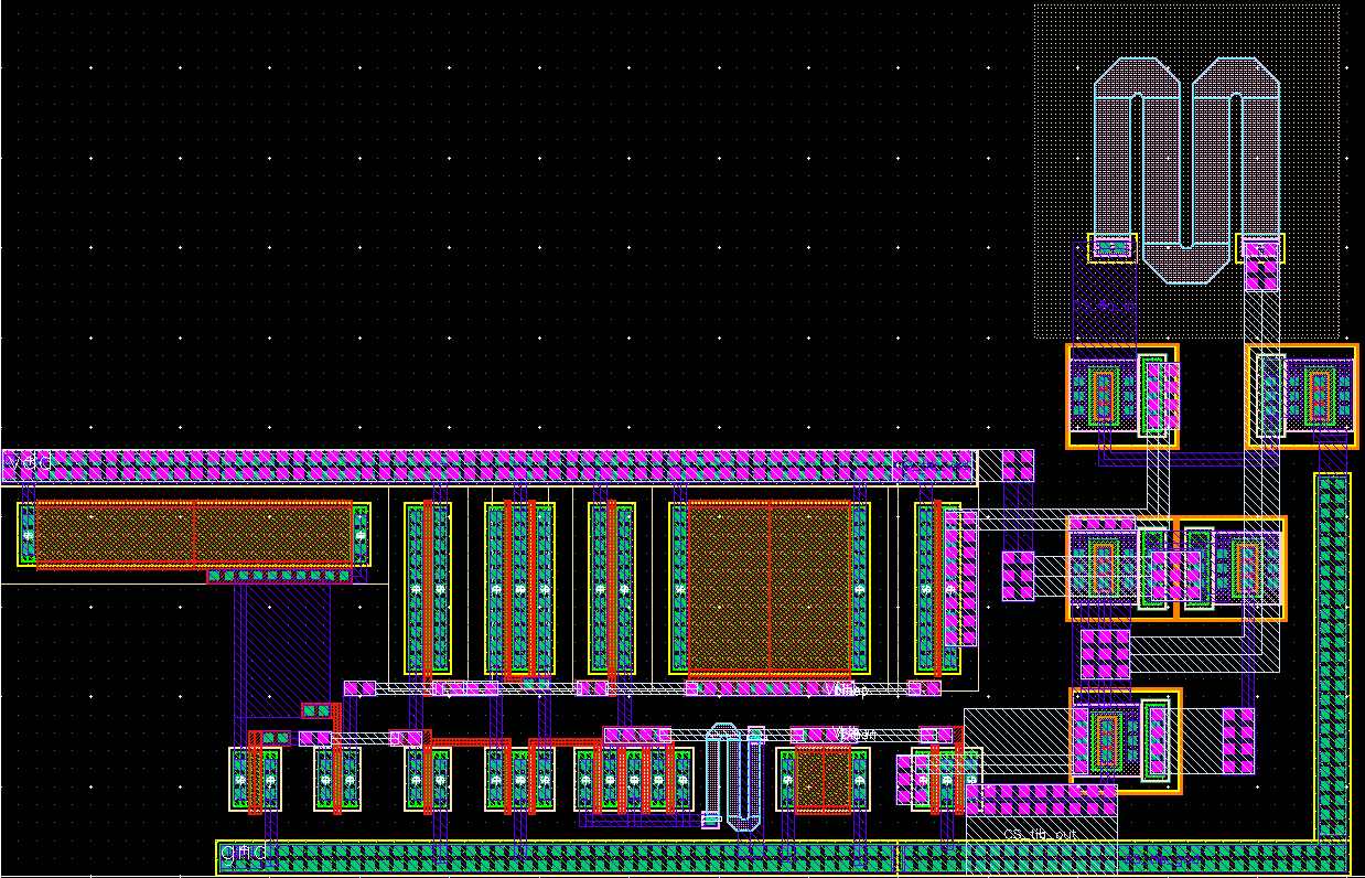
Figure 4: Common Source TIA