Fast Transient Digitizer
Eric Monahan June 5, 2017
Project Members:
R. Jacob Baker (rjacobbaker@gmail.com)
James Mellott (mellott@unlv.nevada.edu)
Eric Monahan (monahan@unlv.nevada.edu)
Angsuman Roy (angsumanroy@gmail.com)
The Fast Transient Digitizer (FTD) is a test chip designed with Cadence Virtuoso and Spectre using On Semiconductor's C5
process. The design was sent for fabrication on June 5, 2017. The design
consists of a 256 stage FTD with an on chip
decoupling capacitor. The main purpose of the FTD is
to sample a high frequency pulse and replicate at a lower frequency enabling
slow read out for analysis.
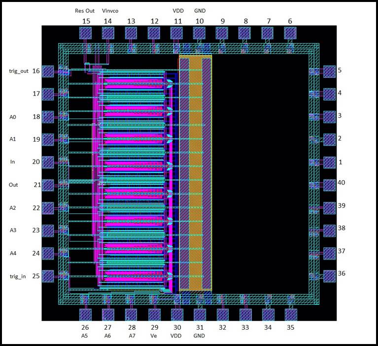
IC PADFRAME AND KEY
PIN TABLE
|
PIN |
NAME
ON KEY |
|
|
1 |
NO
CON |
N/A |
|
2 |
NO
CON |
N/A |
|
3 |
NO
CON |
N/A |
|
4 |
NO
CON |
N/A |
|
5 |
NO
CON |
N/A |
|
6 |
NO
CON |
N/A |
|
7 |
NO
CON |
N/A |
|
8 |
NO
CON |
N/A |
|
9 |
NO
CON |
N/A |
|
10 |
GND |
Ground
Pad |
|
11 |
VDD |
VDD Pad |
|
12 |
NO
CON |
N/A |
|
13 |
NO
CON |
N/A |
|
14 |
Vinvco |
Bias
Generator Control Voltage |
|
15 |
Res
Out |
Bias
Generator Resistor - sets current |
|
16 |
Trig_out |
Output
following 256 stage trigger input signal |
|
17 |
NO
CON |
N/A |
|
18 |
A0 |
Decoder
0 Input |
|
19 |
A1 |
Decoder
1 Input |
|
20 |
In |
Analog
Signal Input Pad |
|
21 |
Out |
Analog
Output Pad to off chip resistor |
|
22 |
A2 |
Decoder
2 Input |
|
23 |
A3 |
Decoder
3 Input |
|
24 |
A4 |
Decoder
4 Input |
|
25 |
Trig_In |
Trigger
Input -starts capturing analog input signal |
|
26 |
A5 |
Decoder
5 Input |
|
27 |
A6 |
Decoder
6 Input |
|
28 |
A7 |
Decoder
7 Input |
|
29 |
Ve |
Enable
Input for decoder |
|
30 |
VDD |
VDD Pad |
|
31 |
GND |
Ground
Pad |
|
32 |
NO
CON |
N/A |
|
33 |
NO
CON |
N/A |
|
34 |
NO
CON |
N/A |
|
35 |
NO
CON |
N/A |
|
36 |
NO
CON |
N/A |
|
37 |
NO
CON |
N/A |
|
38 |
NO
CON |
N/A |
|
39 |
NO
CON |
N/A |
|
40 |
NO
CON |
N/A |
FTD PIN TABLE
|
Component |
Trigger In |
Trigger Out |
Analog In |
Analog Out |
Ground |
|
FTD |
Pin 25 |
Pin 16 |
Pin 20 |
Pin 21 |
Pins 10, 31 |
FTD Flowchart
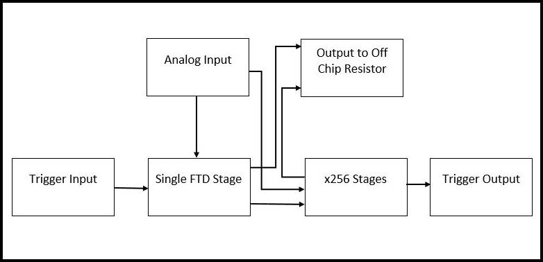
The Fast Transient
Digitizer is a circuit using sequential stages designed to capture high-speed
analog signals via adjustable time intervals that can be read out and analyzed
at a slower speed. The adjustable time intervals for this design vary across a
range from 0.929ns to 6ns
per capture stage. The captured signal is retrieved using a simple decoder that
can access any stage of the circuit at a given time allowing the analog signal
'strength' at that time to be determined. The catalyst for the above FTD design is the Transient Digitizer
Integrated Circuit Design.