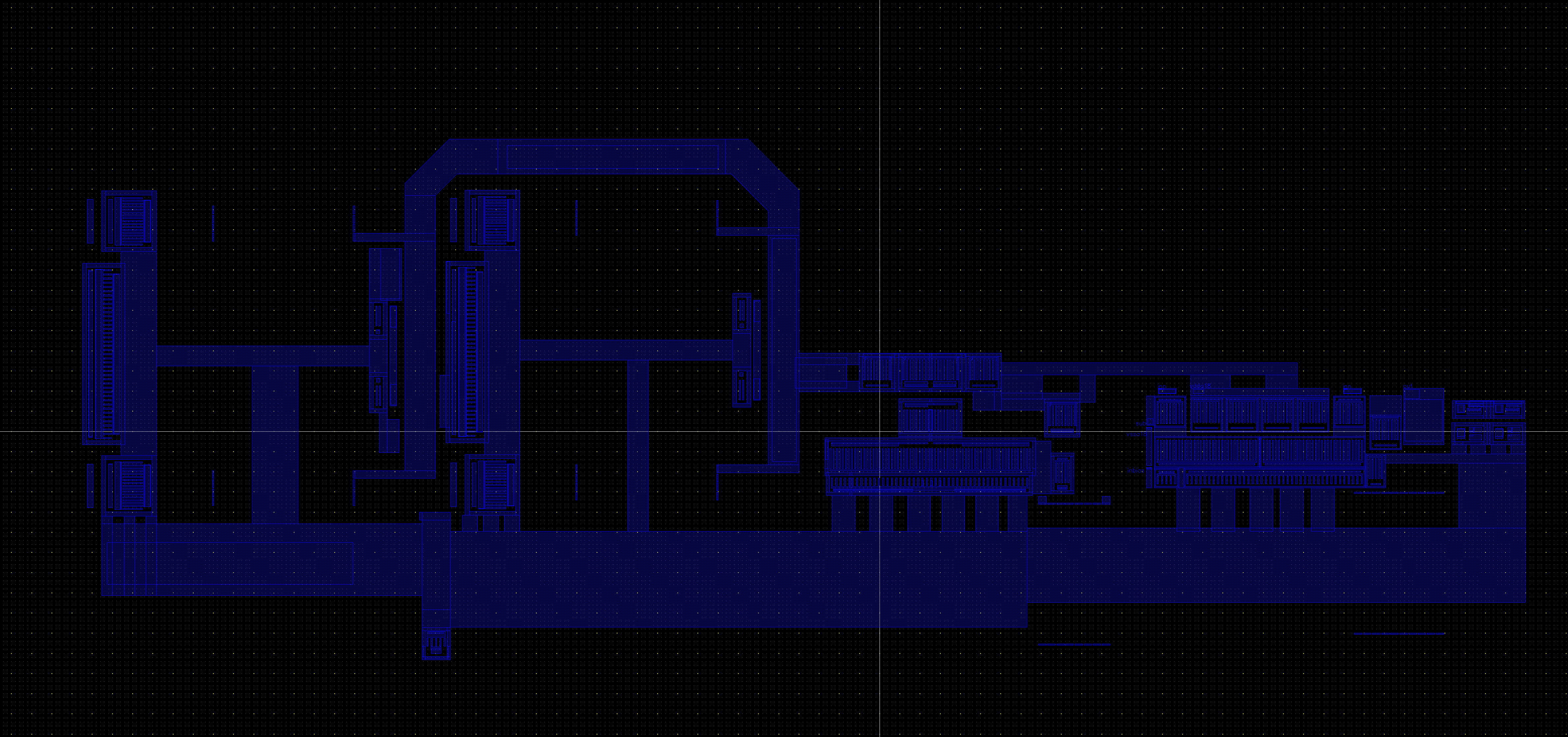
The Analog Chain Layout
Date: 01/06/20
Last Edited on
01/07/20 at 4:25pm using Word
Wiring it all
up:
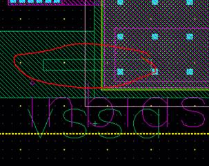
NOTE: Do NOT Wire any pin under a capacitor. The
LVS will register a pin as unbounded (wont see the
pin) if you instantiate below the ablb
layer
Place pin
Here:
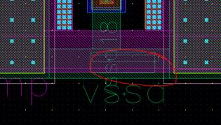 or
or 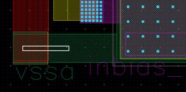
Do NOT place
it here:
 or
or 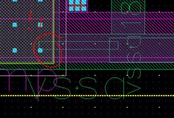
Sub/VDD plane:
Click here to see the layout
VSS plane:
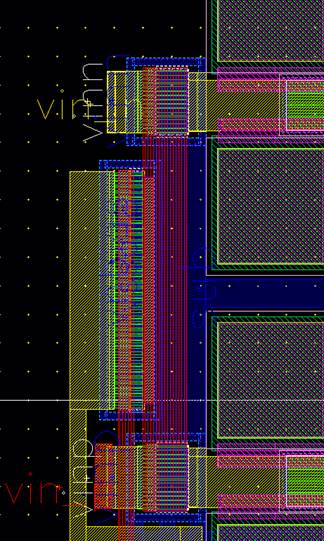
Inputs:
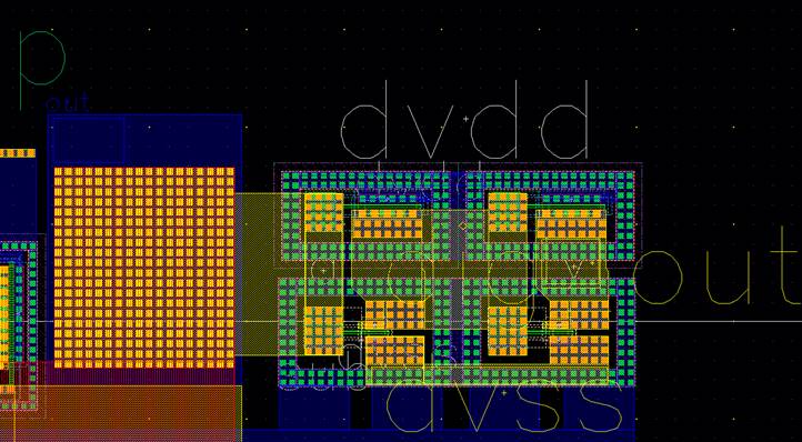
Buffer stage:
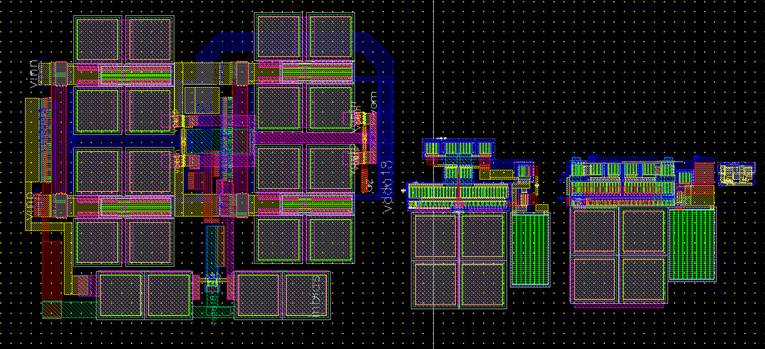
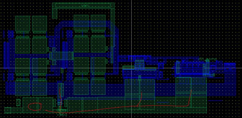
Final Layout:
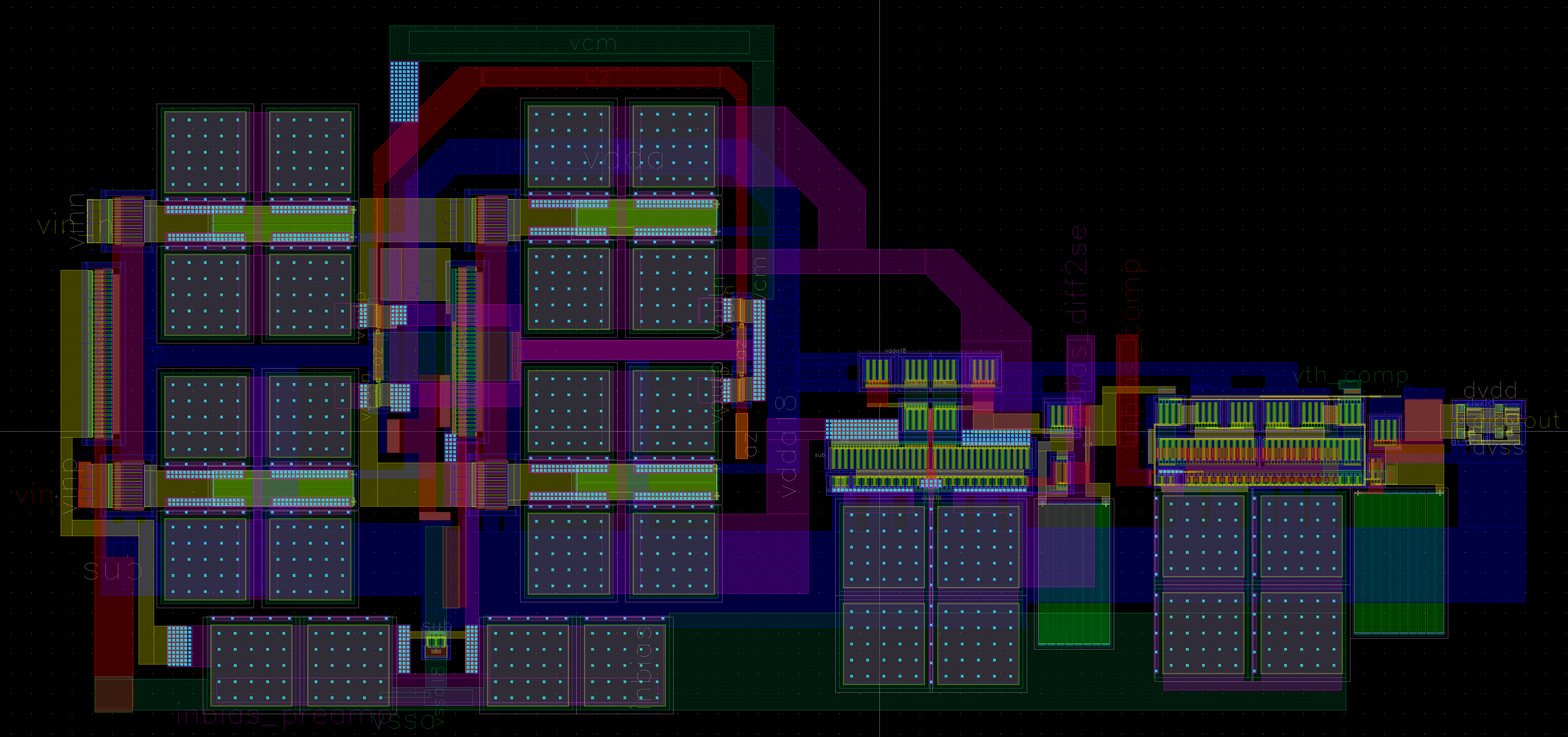
Click here to see the final layout
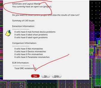
LVS: