An ADC Hierarchy Tutorial in TowerJazz
Date: 01/02/20
Last Edited on
01/03/20 at 6:29pm using Word
So for this layout, we will start with the SH cell. This is the most
important cell in the four levels of hierarchy, as it is instantiated in ALL
levels.
The goal will
be to try to make this cell as user-friendly as possible, and
also trying to make the substrate pins and VDD pins accessible from all
angles.
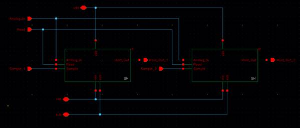
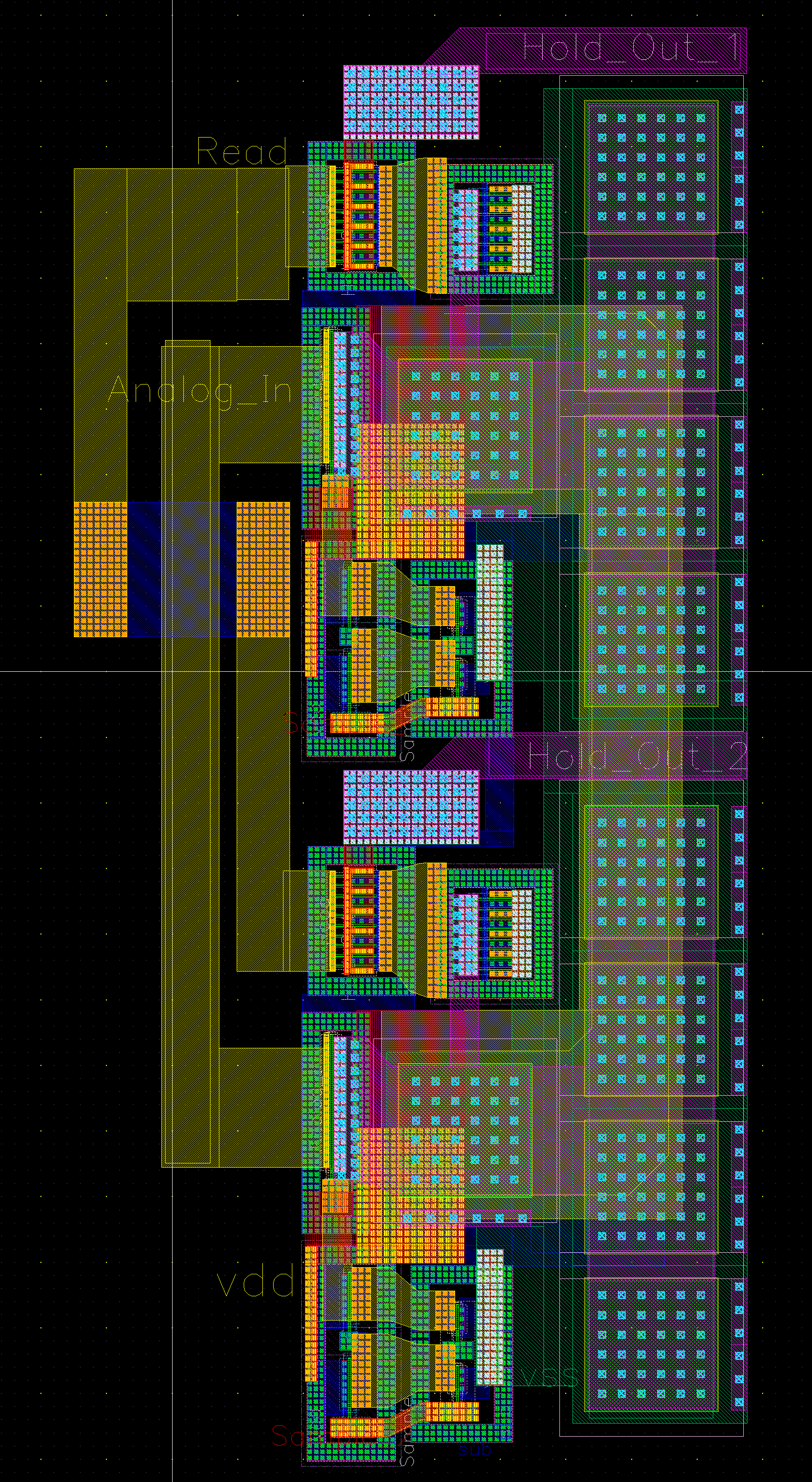
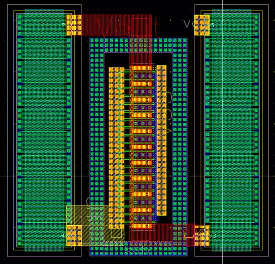
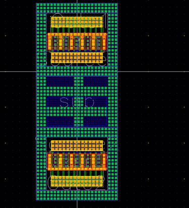
Lets begin with the SH Cell
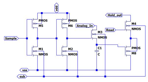
The beginning
is a buffer stage, something that we have already laid out.
The goal will
be trying to make the 2nd stage inputs/outputs accessible.
Here is the
layout:
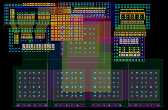
Click here for a high resolution
pic
--------------------------------------------------------
Second Level Hierarchy:
The reason we
spent so much time making the first cell user friendly is so that it will be
easier to instantiate this cell in future layouts.
This next
layout did not take much time to wire at all.
Final Layout:
Click here for a high resolution
pic
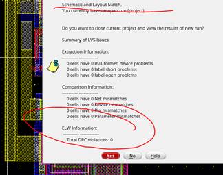
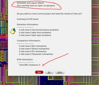
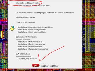
LVS:
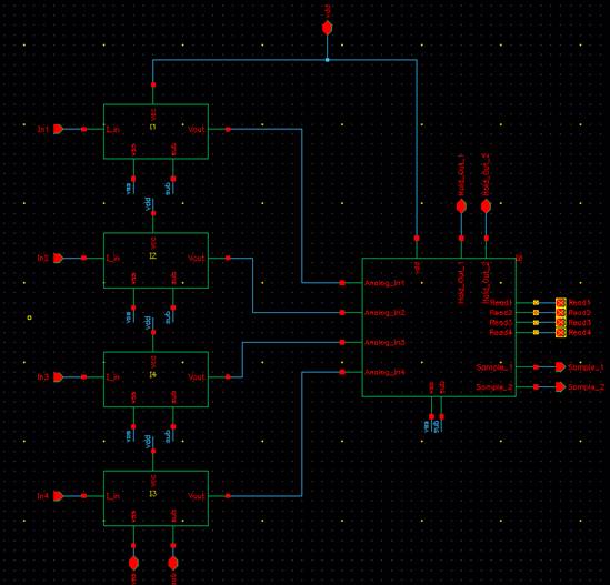
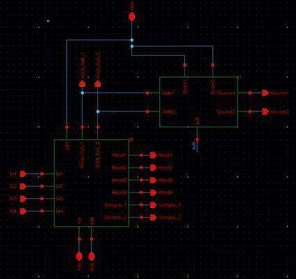
Third Level Hierarchy:
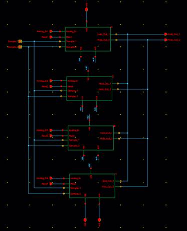
Now, lets wire up the next hierarchy:
The goal of
the entire beginning of making the layout user friendly will definitely
shine here.
Final Layout:
Click here for a high resolution
pic
LVS:
------------------------------------------------------------------------------
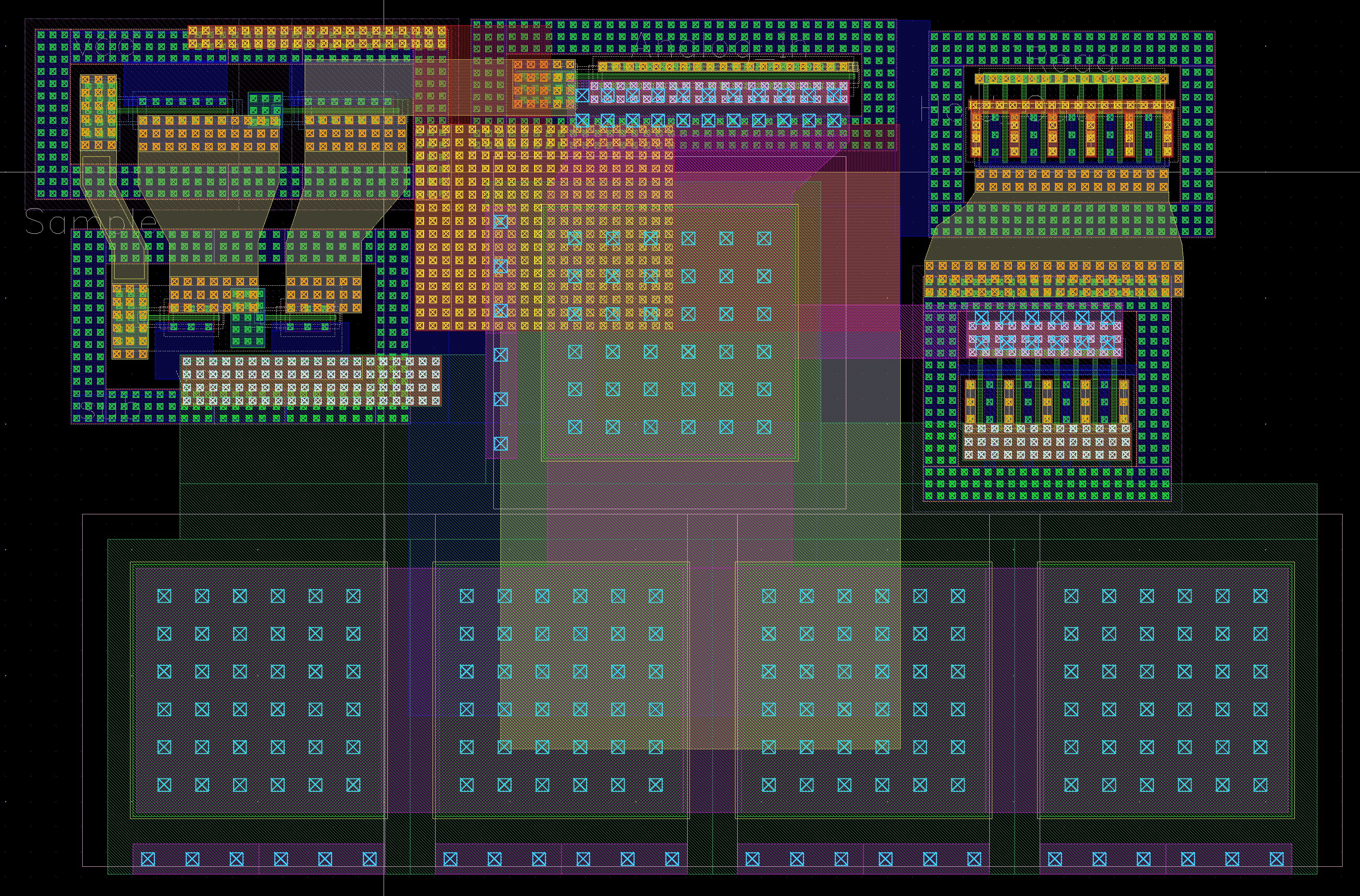
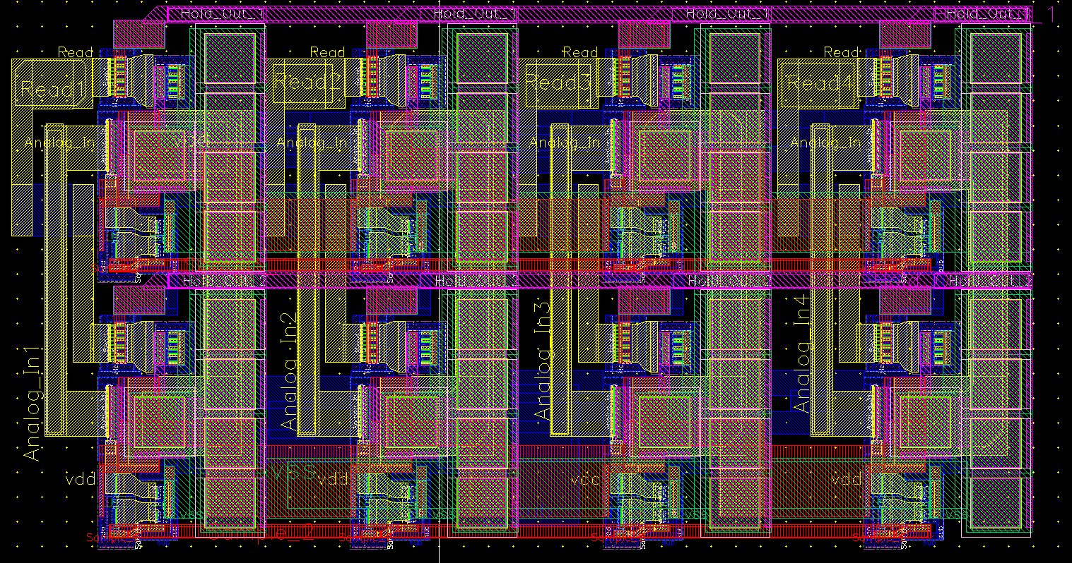
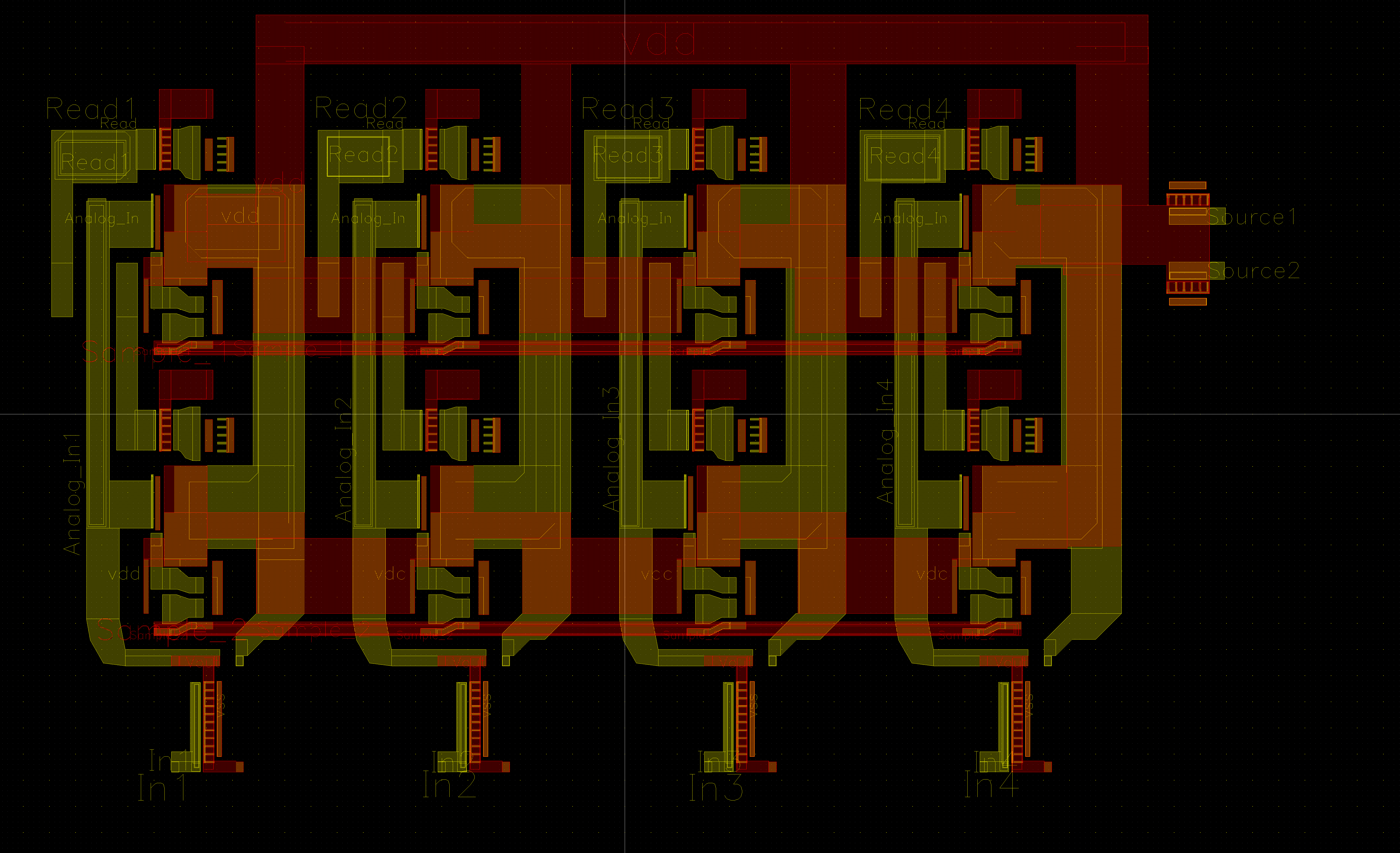
Fourth Level Hierarchy:
Now, for this,
we will be using one instance of the third level layout and four instances of a
Gate-Drain TIA.
Creating the TIA:
Now, placing
this cell into our fourth level hierarchy layout:
Final Layout:
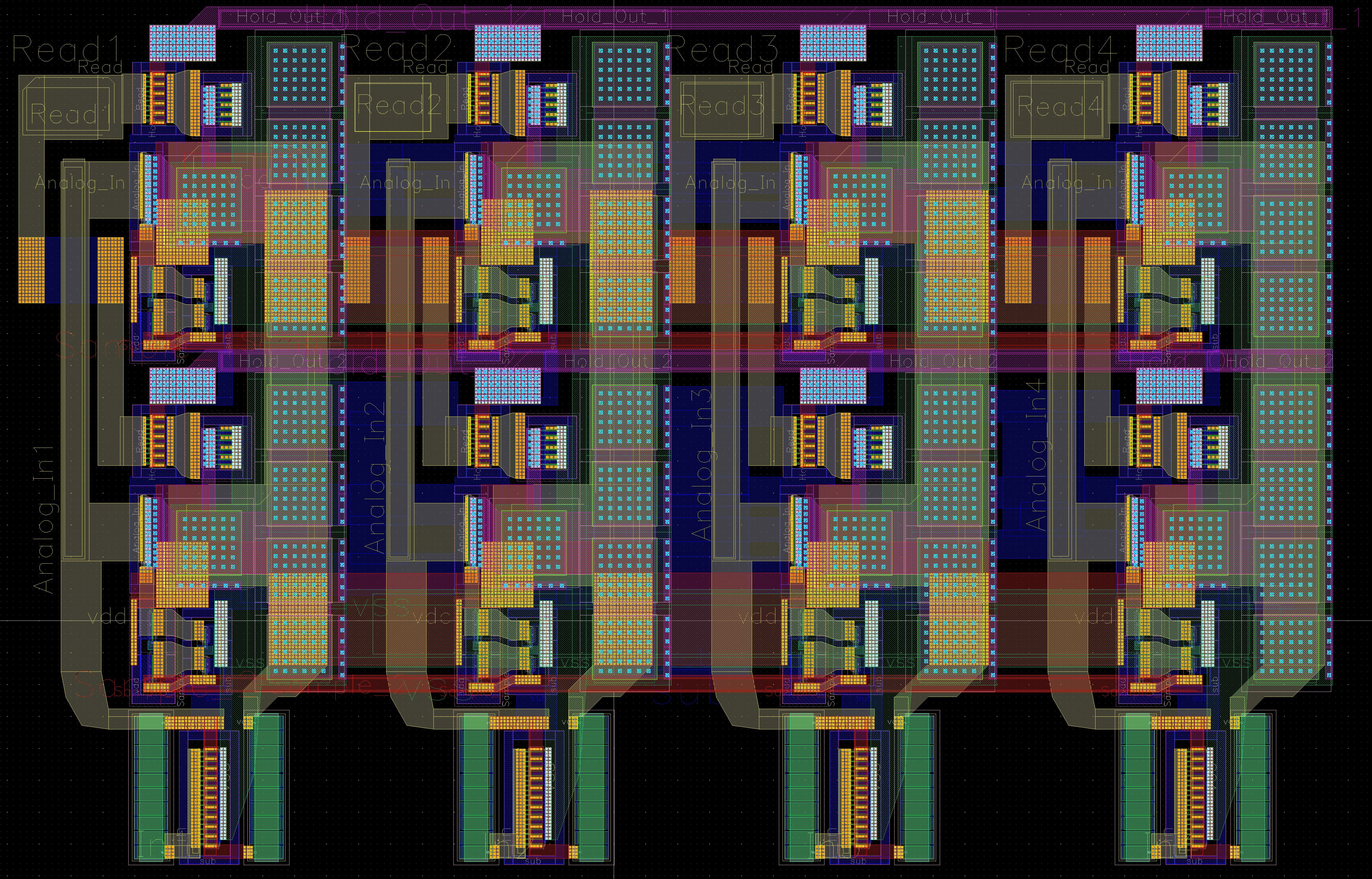
Click here for a high
resolution pic
LVS:
--------------------------------------------------------------
Fifth (Top) Level Hierarchy:
For this
layout, we will use the fourth level layout and connect it with a small source
follower.
Layout of a
simple source follower:
VDD plane:
Click here for a high
resolution pic
VSS Plane:
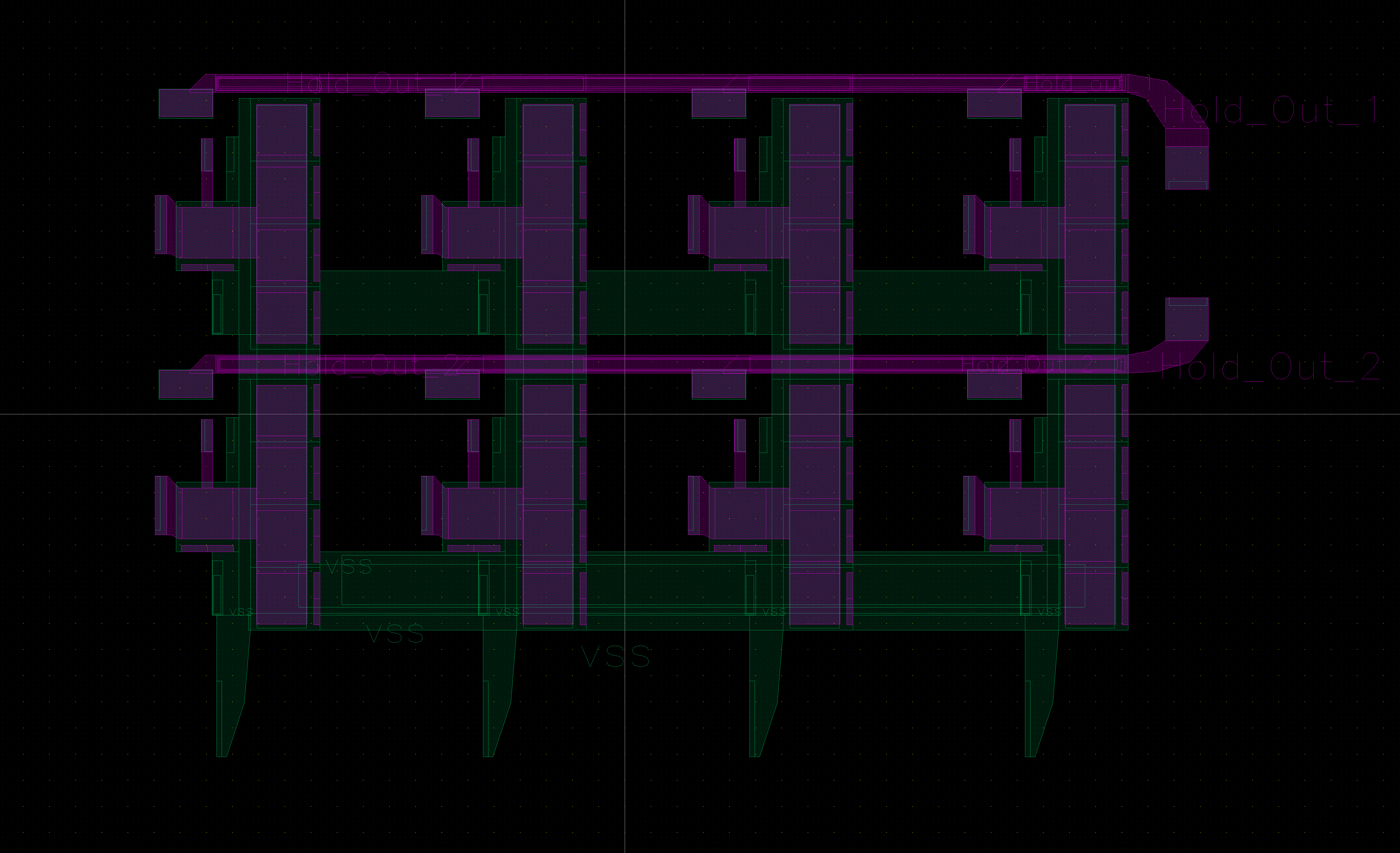
Click here for a high
resolution pic
Sub Plane:
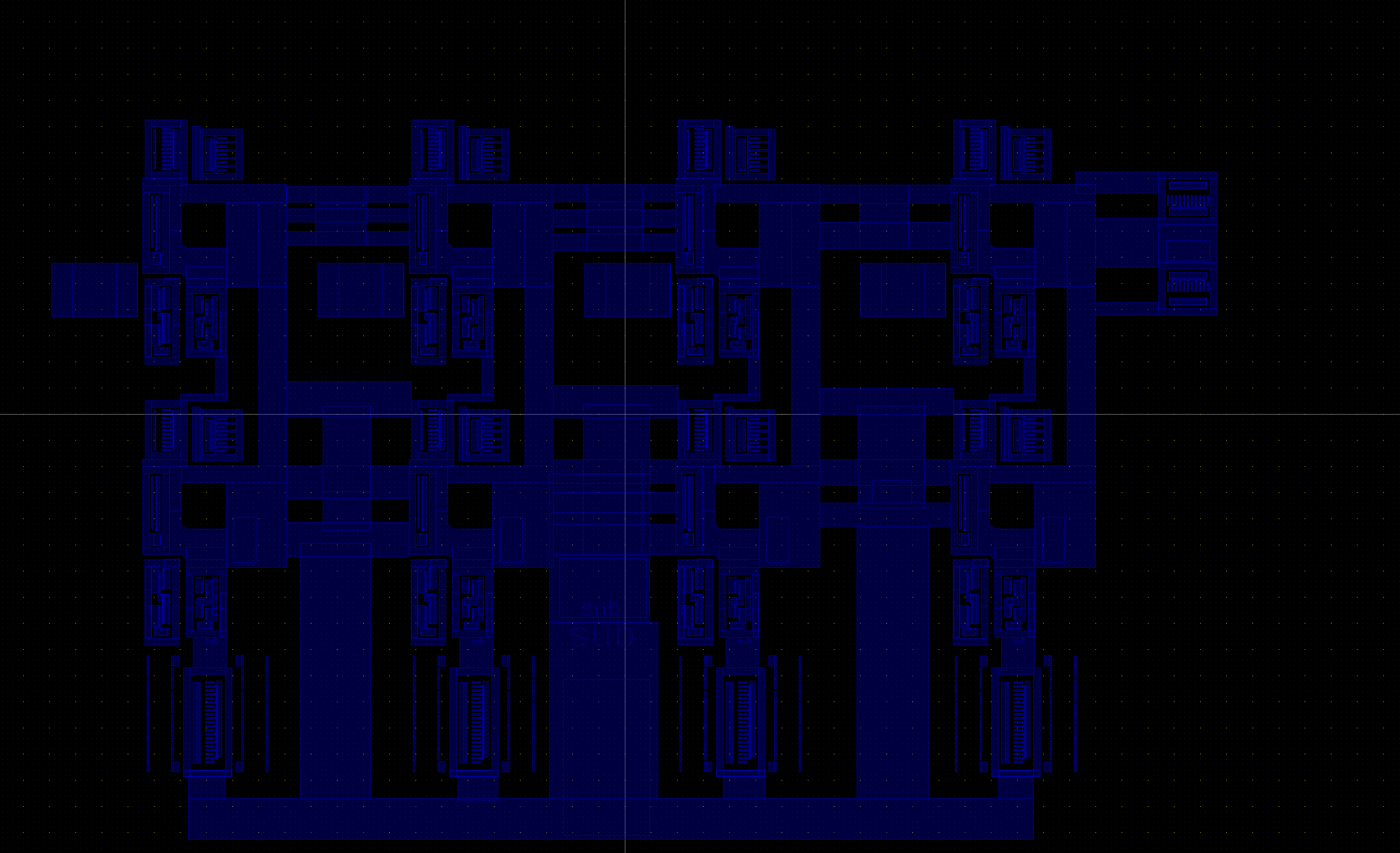
Click here for a high
resolution pic
Final Size:
158μm x 225μm, 17 pins
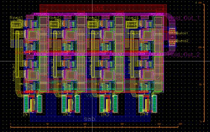
Final Layout:
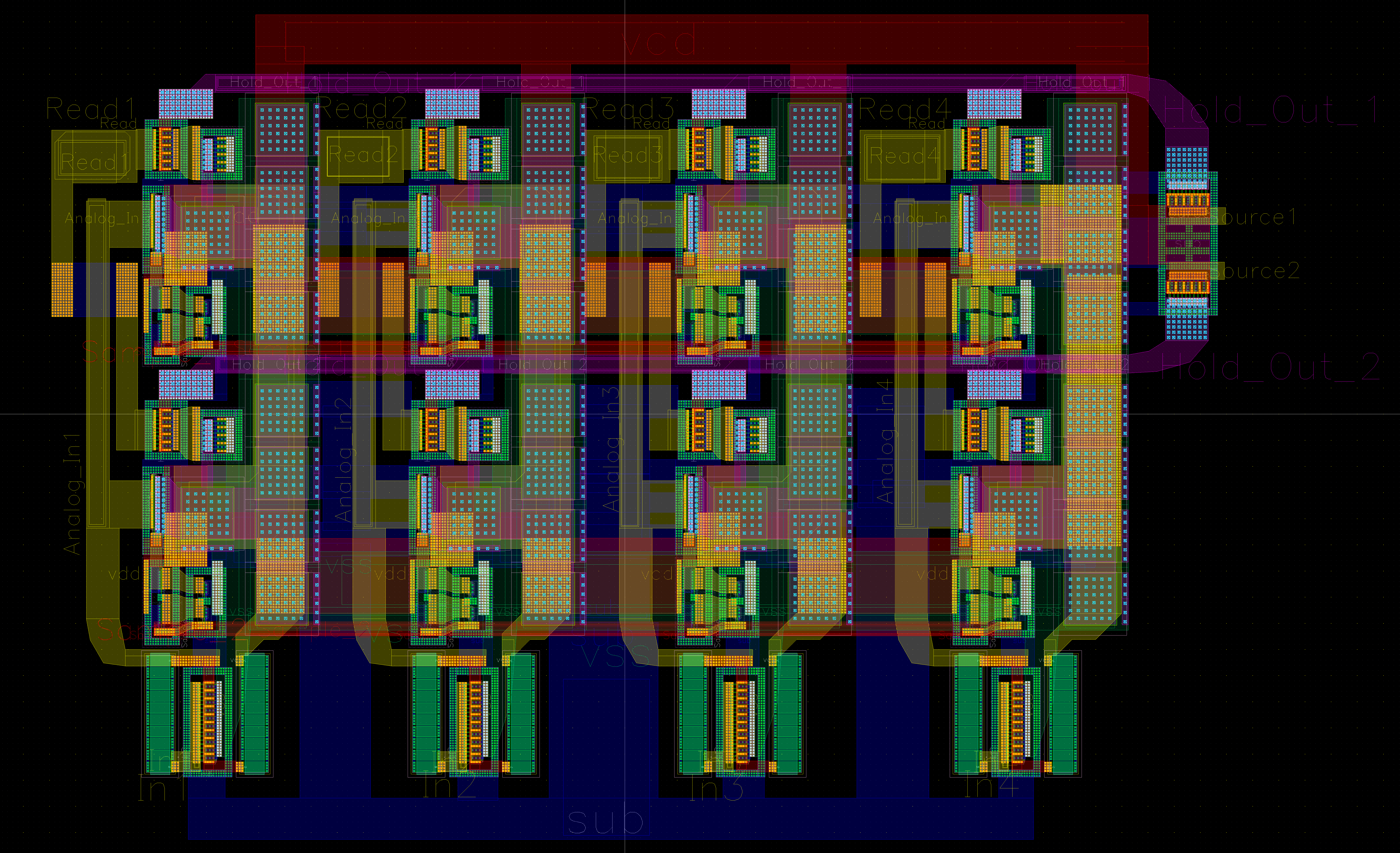
Click here for a high resolution pic
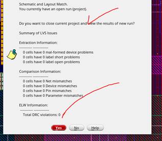
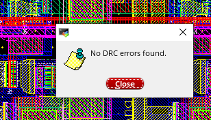
Final DRC:
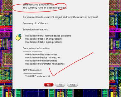
Final LVS:
This completes
the Hierarchal design of an ADC.