![]() TMS Boards
TMS Boards
Daniel’s
PCB Designs
Designed for: Dr. Hines Research Group
About
·
These PCBs were designed for
Transcranial Magnetic Stimulation (TMS) research carried out by Dr. Hines’s
research group. More information about TMS can be found on Daniel’s TMS
research page.
·
TMS circuit are high voltage
circuits, therefore all the following boards are designed with extra thick
traces to increase longevity of the boards.
·
Once the PCBs were received
from manufacturing, Daniel soldered and populated the boards. A few of the
finished boards can be seen on Daniel’s PCB Assembly page.
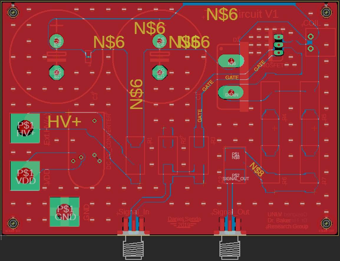
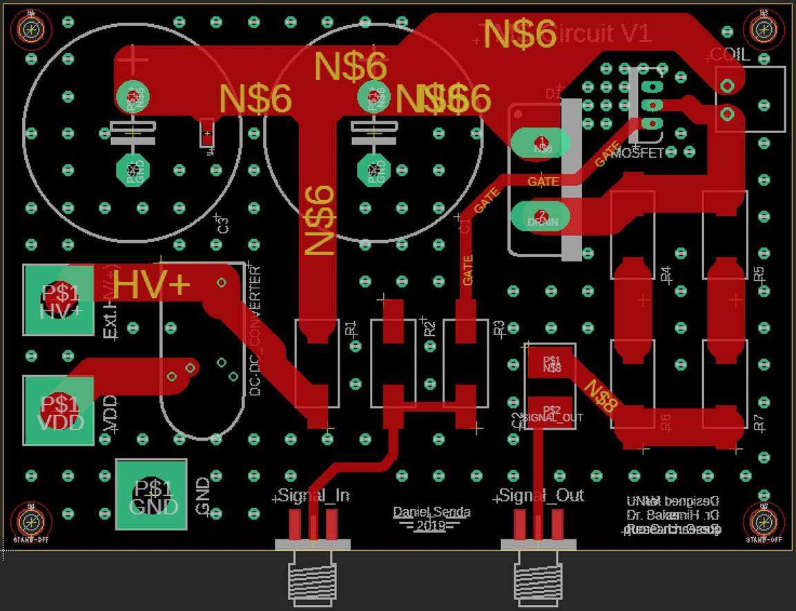
TMS V1
TMS V1 was the first board created
for TMS research. It was designed to have the capability to run on a single
power source and single pulse generator (configured function generator in our
case). It also has the option to add an external high voltage (HV) power supply
instead of using the on-board DC to DC converter. In addition, it has a
dedicated output for easier testing. All the passive components selected for
this design are rated for the high power required for TMS tests. The downfall
to TMS V1 was that it was not designed for a high enough voltage.
Dimensions:(2.95 x 4.25 inches)
TMS V1 Design (Shown in Eagle).
TMS V1 design with hidden GND
planes for better trace visibility.
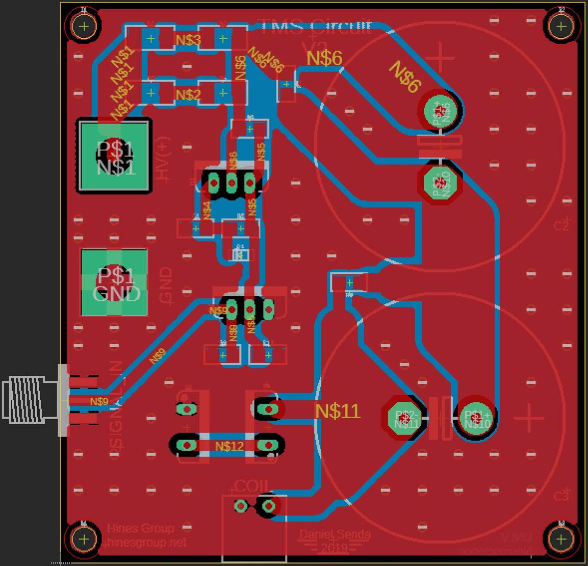
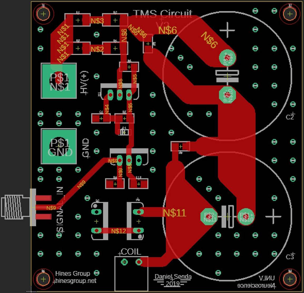
TMS V2
TMS V2 was designed with different requirements in mind. The
major change between V1 and V2 is the addition of another MOSFET. The reason
for doing so was to increase the maximum high voltage that the board can
operate at. Also, research was conducted to find smaller passive components
that were still rated for the high voltage used in TMS testing. The goal was to
make a board with a smaller footprint that could outperform V1. The downfall of
this board was that the MOSFETs would burn out when testing at higher voltages.
Dimensions:(3.1 x 2.9 inches)
TMS V2 Design (Shown in Eagle).
TMS V2 design with hidden GND
planes for better trace visibility.
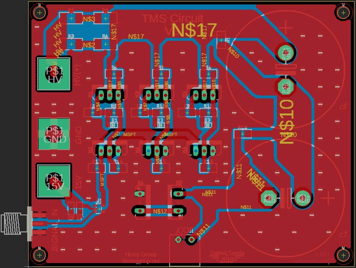
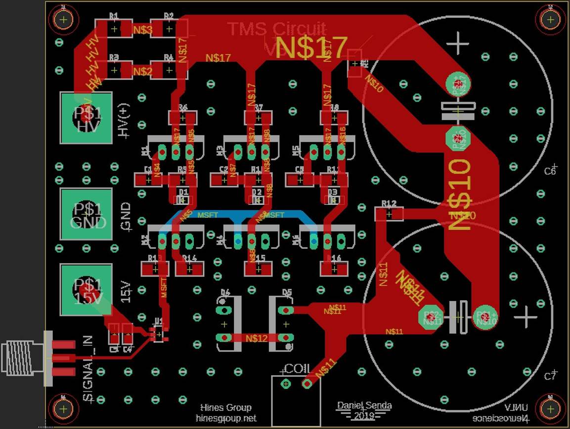
TMS V3
The short comings of TMS V2 were taken in consideration when
designing TMS V3. TMS V3 is like V2, the main difference is that there are
three channels of MOSFETs in order to divide the current flow. By diving the
current flow among three MOSFET channels, we were hoping it would help stop the
burning out of MOSFETs. In addition, V3 has a MOSFET driver to drive all the
MOSFETs on the board. Unfortunately, similar to V2,
the flaw of V3 is that MOSFETs still continued to burn out, although it was at
a slower rate. Dimensions:(3.1 x 3.8
inches)
TMS V3 Design (Shown in Eagle).
TMS V3 design with hidden GND
planes for better trace visibility.
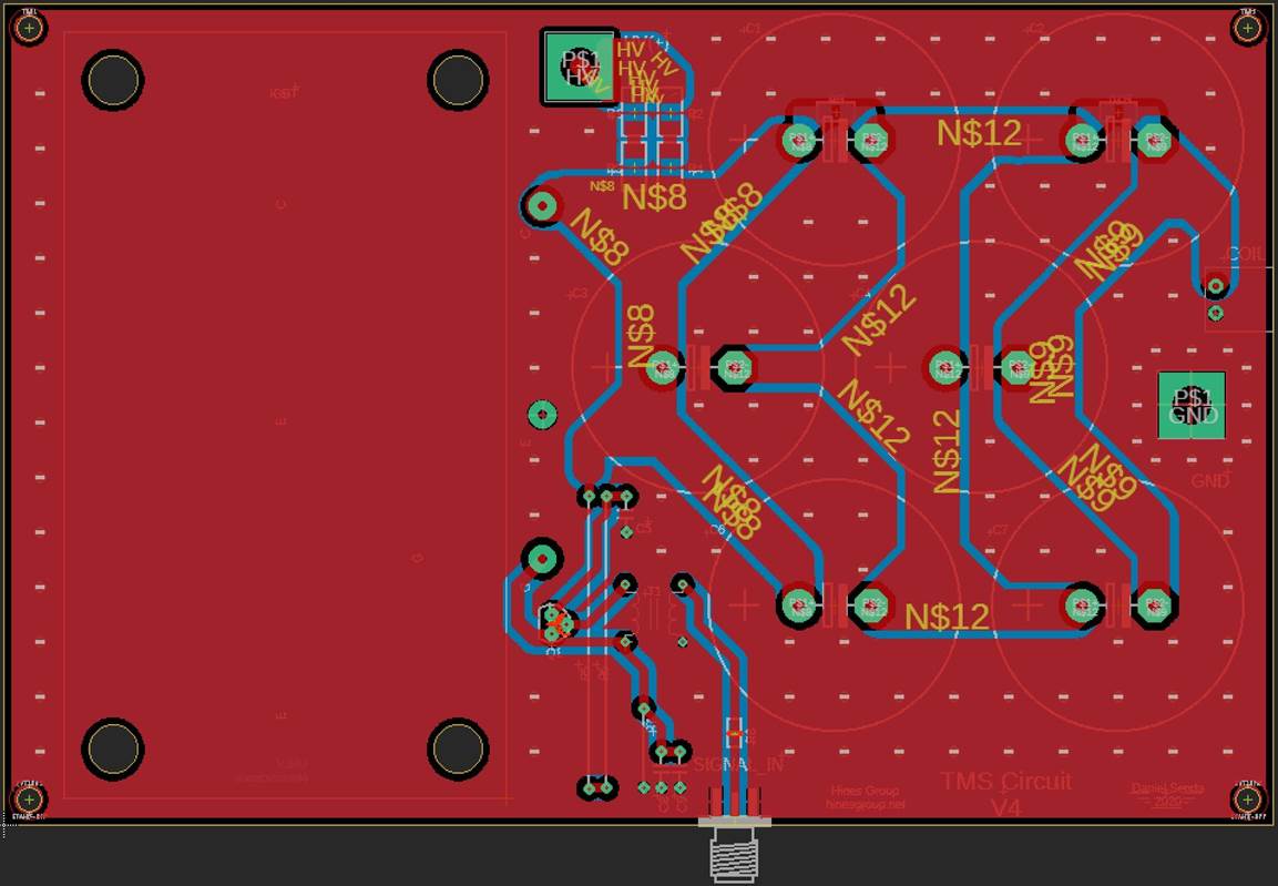
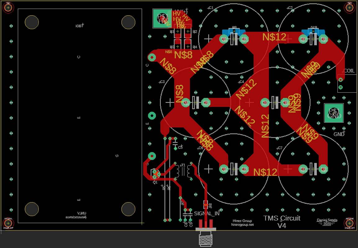
TMS V4 (IGBT)
Using MOSFETs was resulting in undesirable issues, so the
design of V4 revolved around using an insulated-gate bipolar transistor (IGBT)
instead of MOSFETs. IGBTs are designed to be able to handle high voltages and
currents, which is what is needed for TMS testing. To avoid using an additional
voltage supply when operating the circuit, an avalanche transistor was used to
pulse the gate of the IGBT and trigger it. In addition, the board has four
openings to add up to four more capacitors to the circuit if desired. Dimensions:(4.5 x 6.95 inches)
TMS V4 Design (Shown in Eagle).
TMS V4 design with hidden GND
planes for better trace visibility.
Additional Links