Final Project - ECE 421L
Email: yamame1@unlv.nevada.edu
11/22/23
Design a non-inverting buffer circuit that presents less than 100 fF input capacitance to
on-chip logic and that can drive up to a 1 pF load with output voltages greater than 7V (an output logic 0 is near ground
and an output logic 1 is greater than 7V). Assume VDD is between 4.5V and 5.5V, a valid input logic 0 is 1V or less, a valid
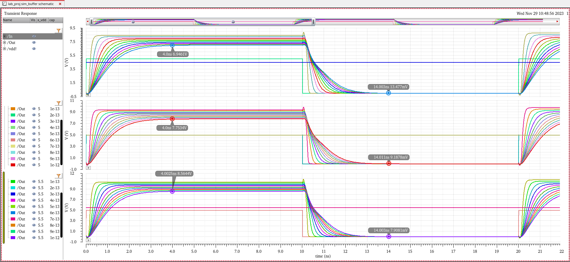
input logic 1 is 3V or more. Show that your design works with varying load capacitance from 0 to 1 pF. Assume the slowest
transition time allowed is 4 ns.
For this project we must output a voltage that is greater than VDD. This necessitates the use of a charge pump.
Part 1 - Schematics and Design
C_in < 100fF)
Cox = Cox’ *W*L*(scale^2) = (2.5fF/um^2) *W*L = 2.5f *W*L
C_in = 3/2(Coxn + Coxp) = 3/2((2.5f *Wn*Ln) + (2.5f *Wp*Lp))
3/2((2.5f *Wn*Ln) + (2.5f *Wp*Lp)) < 100f
3.75f((Wn*Ln) + (Wp*Lp)) < 100f
*Using 24/12 inv
3.75f(((12)*(0.6)) + ((24)*(0.6))) < 100f
81f < 100f
tp < 4ns)
R’n = 20kΩ, R’p = 40kΩ
R = R’ * L/W
tp = 0.7 * R * C_L
tp = 0.7 * R * 1pF
0.7 * R * 100pF < 4n
R < 5.7kΩ
Designing for conditions beyond spec. We will select R = 1.5k
Rn = 20k *Ln/Wn = 1.5k -> 3/40 -> 3/42 -> 1/14 = Ln/Wn
Rp = 40k *Lp/Wp = 1.5k -> 3/80 -> 3/81 -> 1/27= Lp/Wn
To use minimum lengths lets use
-> Wn/Ln = 14/1 -> 8.4u/0.6u
-> Wp/Lp = 27/1 -> 16.28u/0.6u
t_pHL = t_pLH = 0.7 * 1.5k * 1p = 1.05ns = tp
tr = 2.2 * 1.5k * 1p = 3.3ns
Vout > 7V)
Since
we can expect to get 2Vdd at our output at the lowest Vdd of 4.5V this
condition should be met but we must size our large capacitor (Cx)
appropriately.
To properly size our capacitor we can use the basic relationship of Q = CV.
Using
a simple charge sharing circuit to do this analysis with CL and Cx we
can say that the charge of the sharing ckt when the switch is open
(Q_a) is equal to the charge of the ckt when the switch is closed
(Q_b).
Q_a = (CL + Cx)*Vout
Q_b = Cx * 2Vdd
-> Q_a = Q_b
-> (CL + Cx)*Vout = Cx * 2Vdd
Vout = (Cx * 2Vdd)/(CL + Cx)
Given that Vdd >= 4.5V and Vout must be >= 7V
7 <= (Cx * 9)/(1p + Cx)
-> 7/9 <= Cx/(10^-12 + Cx)
->7*(10^-12 + Cx) <= 9*Cx -> Cx >= (7*10^-12)/2 = 3.5pF
Designing past the given specs we will choose Cx = 5pF
*using moscaps over poly-poly capacitors for layout ease.
Sizing moscaps)
100f = 2.5f *W*L
40 = W*L = W^2 -> sqrt(40) = 6.32 ~= 6.3 for staying on grid
100f -> 6.3u/6.3u
5p = 2.5f *W*L
2k = W*L = W^2 -> sqrt(2000) = 44.72 ~= 44.7
5p -> 44.7u/44.7u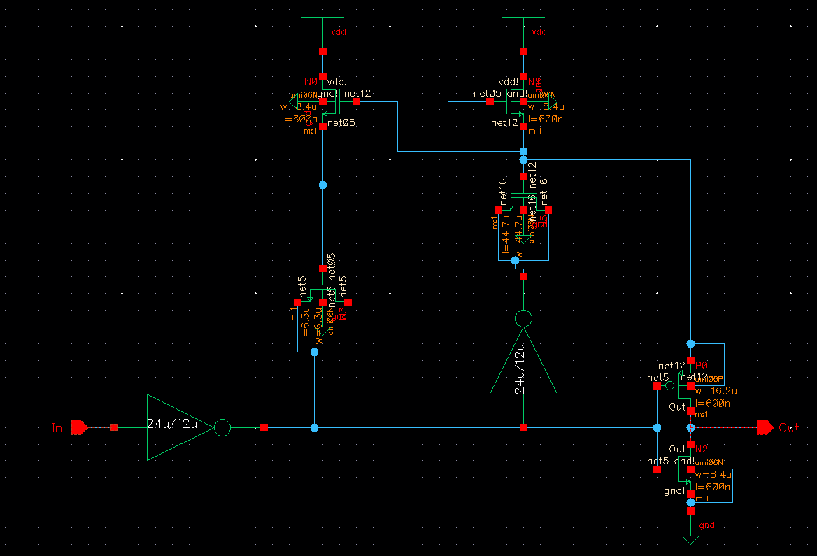
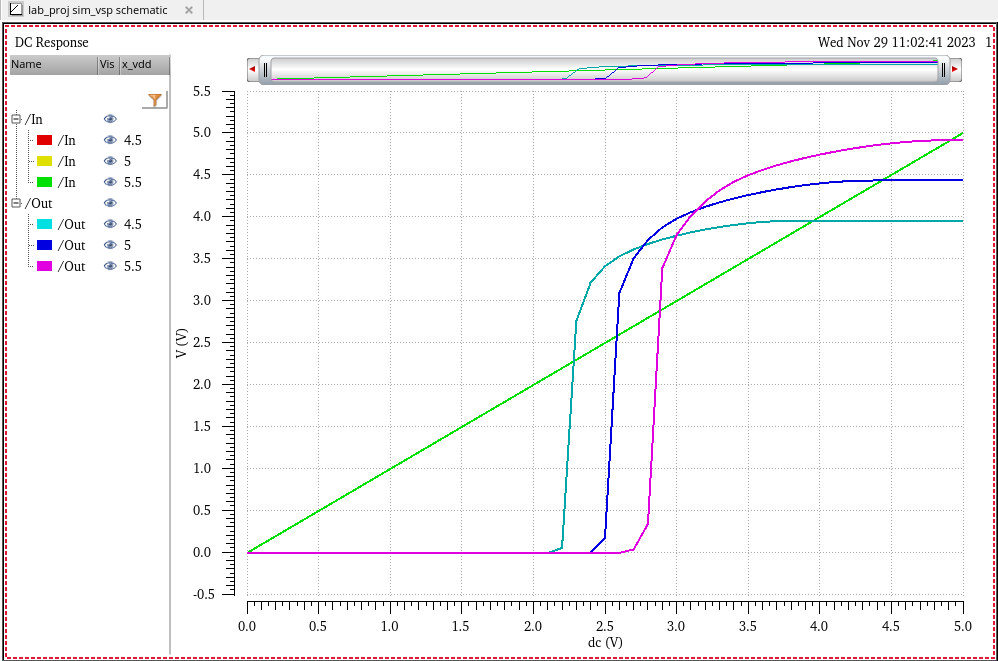
Varying Cap and vdd)
VSP)
We can see that for all cases our Vsp sits between 2.25V and 2.75V
Part 2 - Layout
For the second part of our project we must layout the circuit described in our schematic.
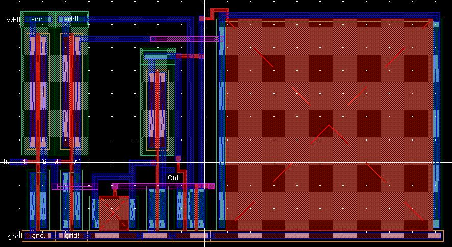
For our design, we only have four pins, those being In, Out, vdd! and gnd!. For good practice we used metal1 and metal2 for most connections and only used poly1 for local interconnections. As mentioned earlier we used moscaps as opposed to poly-poly capacitors so that we would use less space to layour our device. If we used a poly-poly capacitor for our 5pf, we would require about 74.5um^2 which is approaching double the space needed for our moscap.
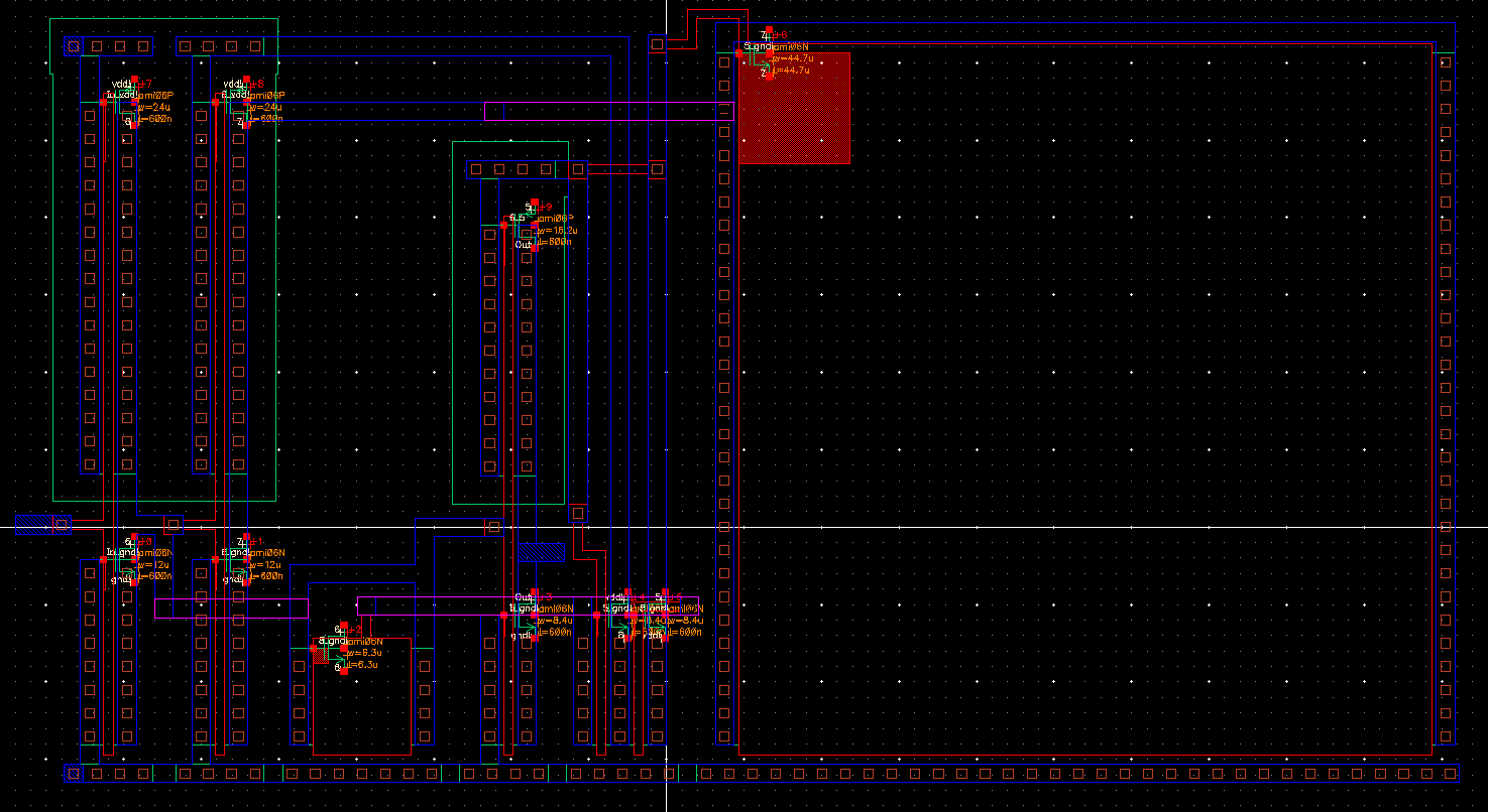
Here we can see my layout and the resulting extracted view of the layout.
One thing to note is that it is important to seperate the third PMOS so that the body is not connected to VDD.
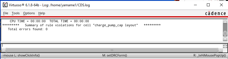
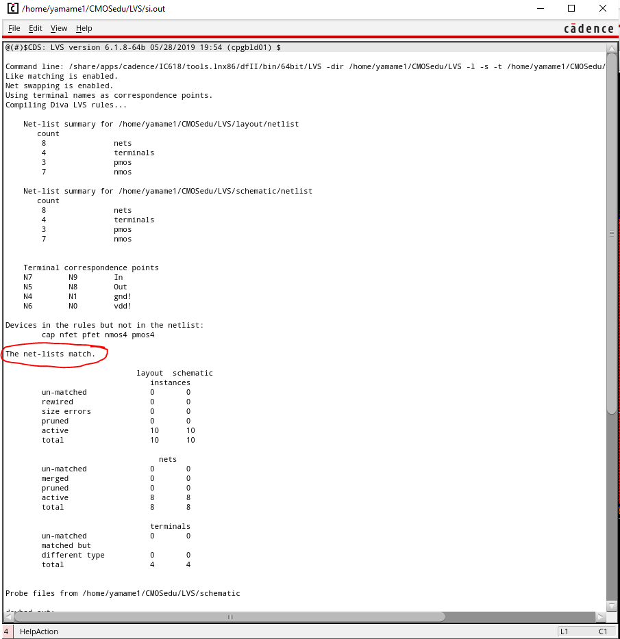
As we can see, our layout cleanly passed the DRC and LVS.
Now we know that our design can be fabricated.
As always I backed up my work, and I will include my design directory here.
This
concludes this project demonstrating how to design and layout a
non-inverting buffer circuit within the given parameters.