Lab 8 - ECE 421L
In this lab, we take our final project and place it onto a chip along with other components to help give the chip additional functionality:
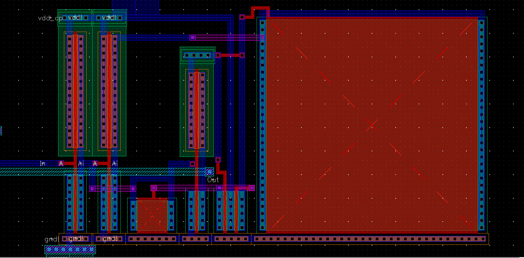
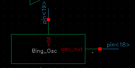
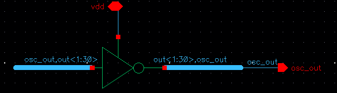
We took Ethan's course project for this lab, and put it on the chip. Here is a picture of ethan's layout and schematic
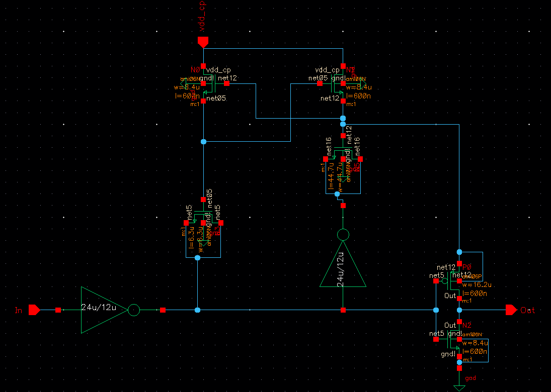
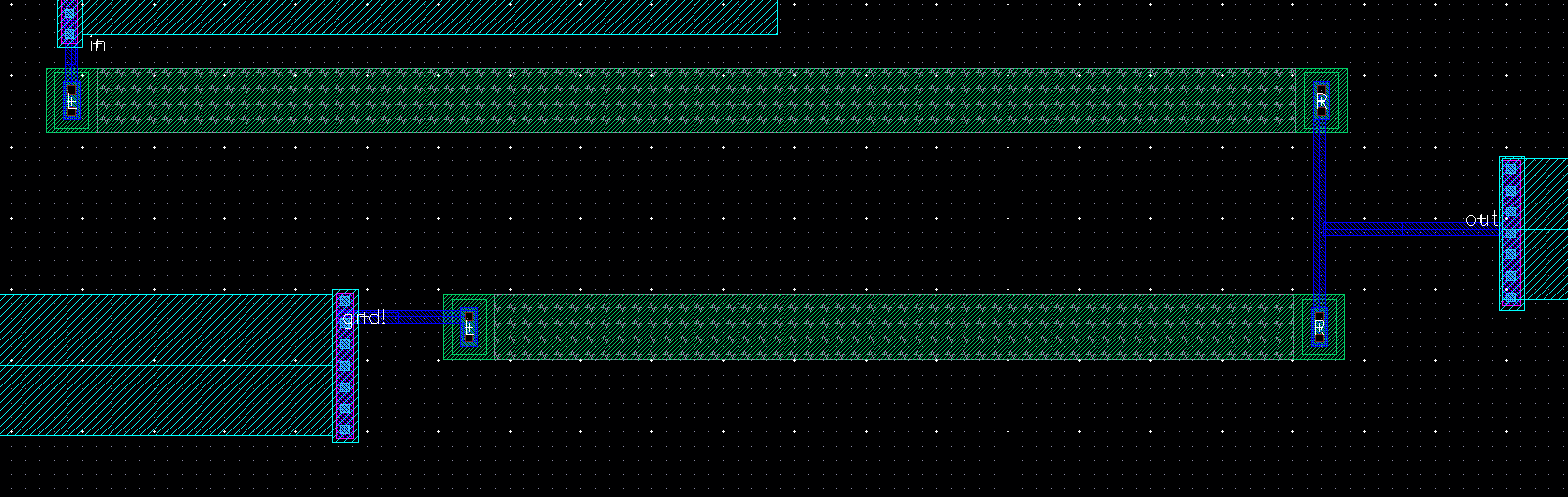
This is the schematic and the layout of the ring oscillator. It drives a 20pF load capacitor.
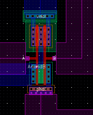
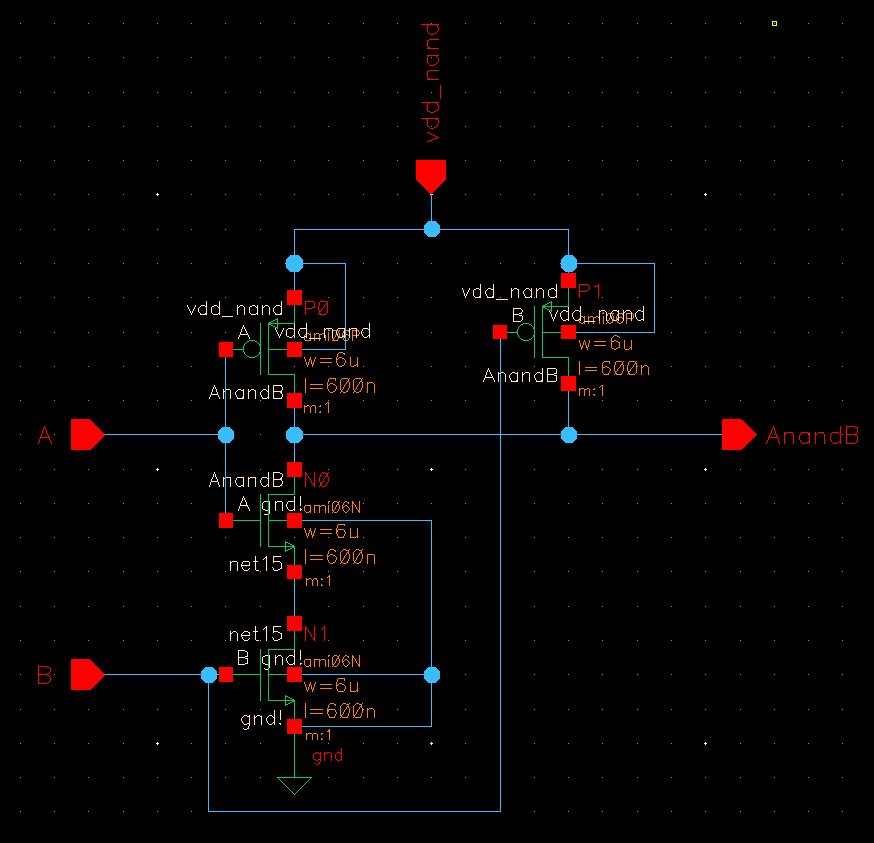
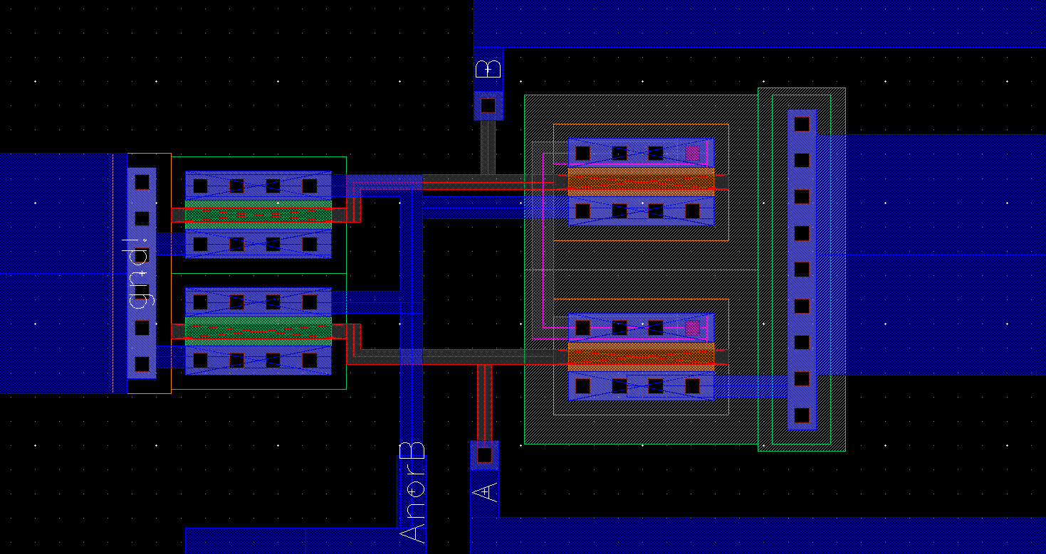
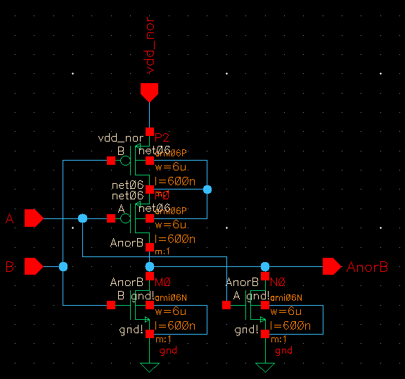
NAND and NOR gates using 6/0.6 NMOSs and PMOSs (1 point)
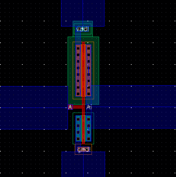
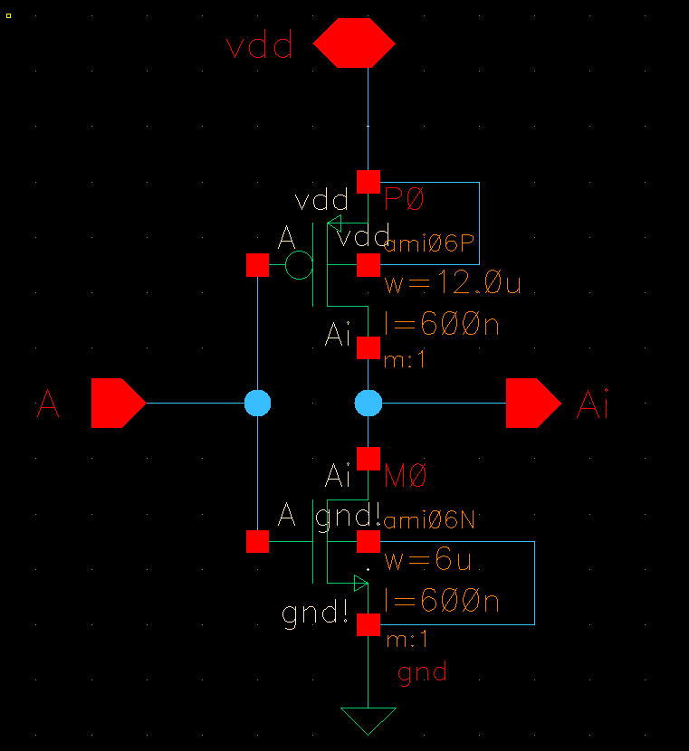
An inverter made with a 6/0.6 NMOS and a 12/0.6 PMOS (1 point)
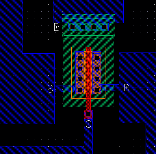
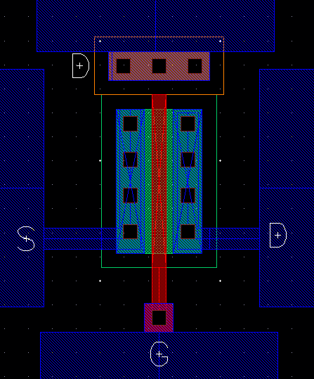
Transistors, both PMOS and NMOS, measuring 6u/0.6u where all 4 terminals of each
device are connected to bond pads (7 pads + common gnd pad) (1point)
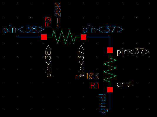
Using the 25k resistor laid out below and a 10k resistor implement a voltage
divider (need only 1 more pad above the ones used for the 25k resistor) (1 point)
A 25k resistor implemented using the n-well (connect between 2 pads but we also need a common gnd pad) (1 point)
This is what the overall padframe ended up looking like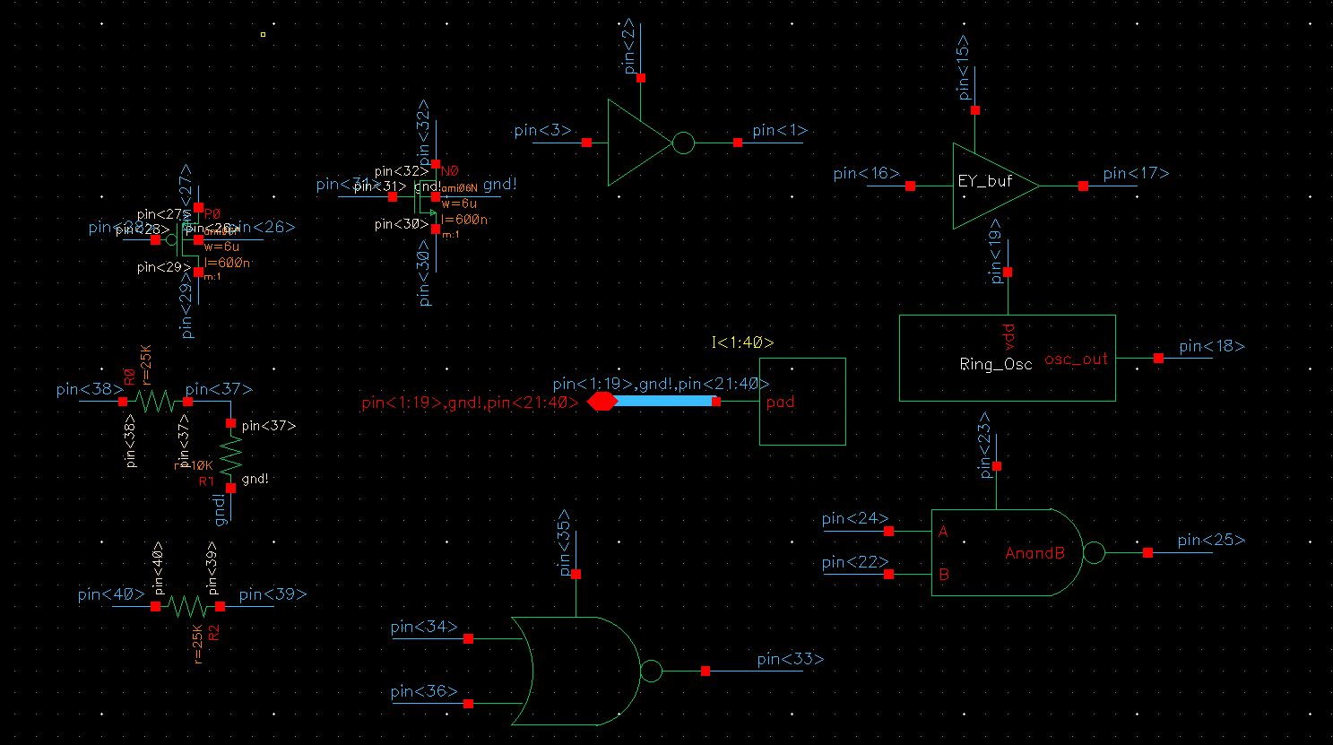
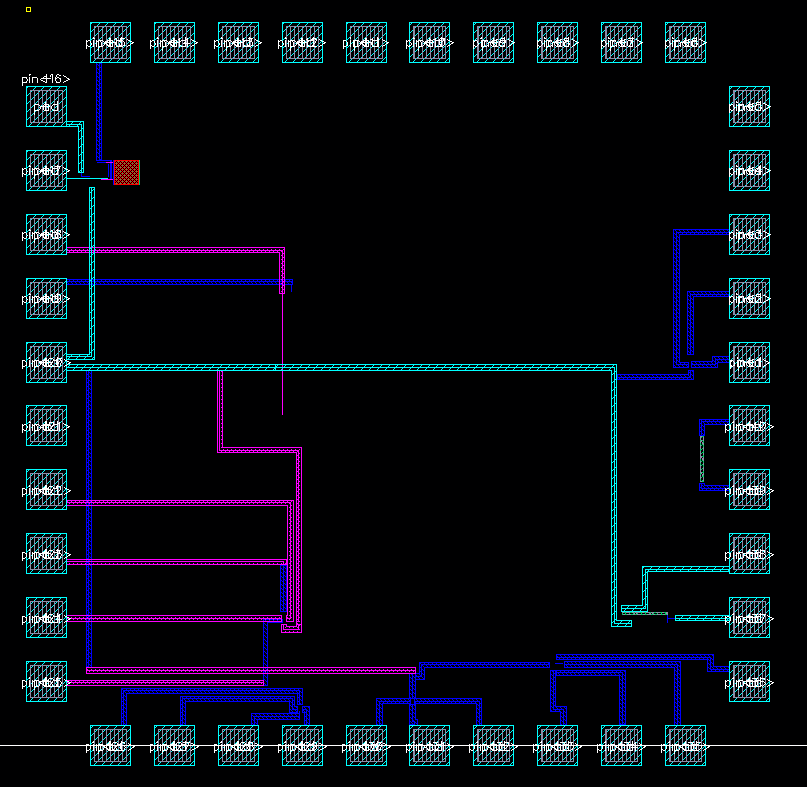
The pinout for the above frame is as follows:
| Pin 1 | INV - out | Pin 11 | NOCONN | Pin 21 | NOCONN | Pin 31 | NMOS - G |
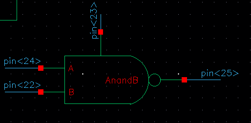
| Pin 2 | INV - vdd | Pin 12 | NOCONN | Pin 22 | NAND - B | Pin 32 | NMOS - D |
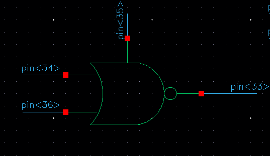
| Pin 3 | INV - in | Pin 13 | NOCONN | Pin 23 | NAND - vdd | Pin 33 | NOR - out |
| Pin 4 | NOCONN | Pin 14 | NOCONN | Pin 24 | NAND - A | Pin 34 | NOR - A |
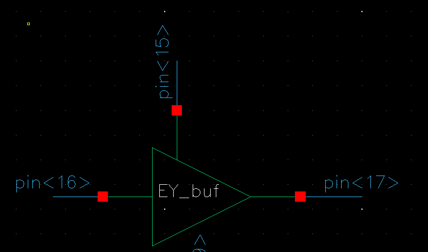
| Pin 5 | NOCONN | Pin 15 | CP - vdd | Pin 25 | NAND - out | Pin 35 | NOR - vdd |
| Pin 6 | NOCONN | Pin 16 | CP - in | Pin 26 | PMOS - body | Pin 36 | NOR - B |
| Pin 7 | NOCONN | Pin 17 | CP - out | Pin 27 | PMOS - S | Pin 37 | RD - out |
| Pin 8 | NOCONN | Pin 18 | RO - out | Pin 28 | PMOS - G | Pin 38 | RD - vin |
| Pin 9 | NOCONN | Pin 19 | RO - vdd | Pin 29 | PMOS - D | Pin 39 | R - in |
| Pin 10 | NOCONN | Pin 20 | gnd!! | Pin 30 | NMOS - S | Pin 40 | R - out |
Simple explanation on how to test each test structure, with simulations (e.g.
What inputs should be given to the circuit? What pin numbers on the
chip should the user connect to?) (2 points)
Before any testing be sure to tie pin 20 to the ground of your Voltage-source, function generator, multimeter or Oscope.
INVERTER) Tie minimum 3v input to pin 3, output should return value under 2v on pin 1. The opposite should also be true. Ensure to tie the vdd to a constant 5v source. This Inverter is capable of driving a 20pf load.Charge Pump) Tie pin 15 to 4.5-5.5V, feed pin 16 <1V for low or >3V for high. The output pin 17 should then show essentially zero or >7V depending on the input.
Ring Oscillator) Tie pin 19 to 5V and watch output change at a specified frequency.
NAND) After tying vdd to 5V vary the inputs according to the table and output change accordingly
Where a logic 1 is above 3V and logic 0 is under 2V
| A | B | Out |
| 0 | 0 | 1 |
| 0 | 1 | 1 |
| 1 | 0 | 1 |
| 1 | 1 | 0 |
NOR) After tying vdd to 5V vary the inputs according to the table and output change accordingly
Where a logic 1 is above 3V and logic 0 is under 2V
| A | B | Out |
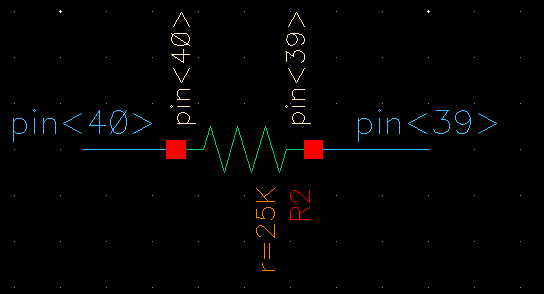
| 0 | 0 | 1 |
| 0 | 1 | 0 |
| 1 | 0 | 0 |
| 1 | 1 | 0 |
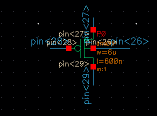
PMOS) Tie connect pin 29 a the drain, connect pin 28 as your gate, body at pin 26 and pin 27 as the source. Test any number of ways but verify it follows the respective equations for the three regions of operation
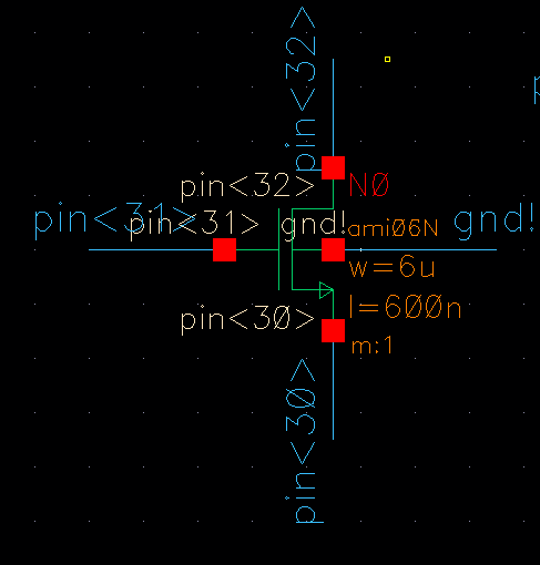
NMOS) Tie connect pin 32 a the drain, connect pin 31 as your gate, and pin 30 as the source. Test any number of ways but verify it follows the respective equations for the three regions of operation. (body is already tied to ground)
Resistive Divider) Tie input to some voltage vin pin38 . The output on pin 37 should be = vin * 2/7
Resistor) pins 39 and 40 can be used as a regular resistor. We can check it using an ohm meter or ohms law
Top level cell chip schematic + layout that is DRC/LVS clean [if available]
and adheres to the instructions given (circuits cannot share power, GND
pin is pin 20, etc) (1 point)
The design directory can be found here, and as always we backed up our work.