Lab 2 - ECE 421L
Email: yamame1@unlv.nevada.edu
9/13/23
Prior to lab, I read the lab, completed the work below and backed up my work.
1) Narrative
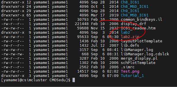
We started this prelab by getting the lab2 file onto our server by uploading and unzipping
it in our project directory as seen in the image below.
After we have our file is uploaded we added "DEFINE lab2 $HOME/CMOSedu/lab2"
to our cds.lib.
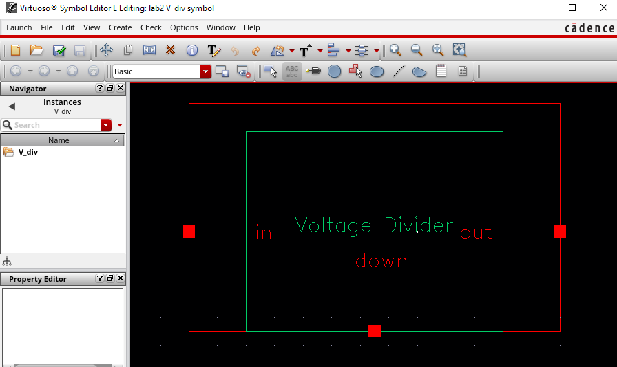
Once that is complete we can access our lab2 folder using Cadence.
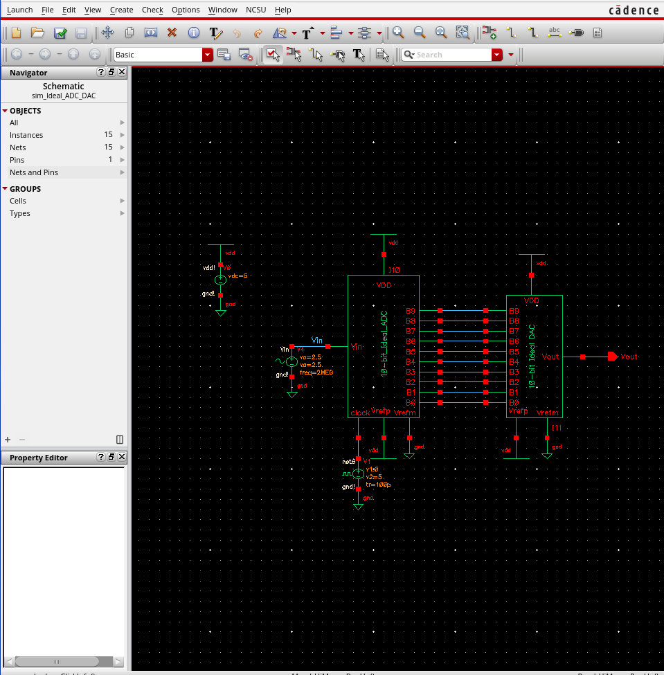
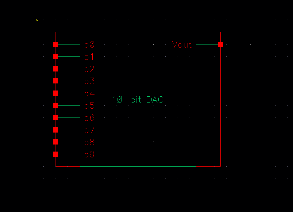
With that said, our next step was to launch cadence and open the
ideal 10-bit ADC and DAC as shown in the following image.
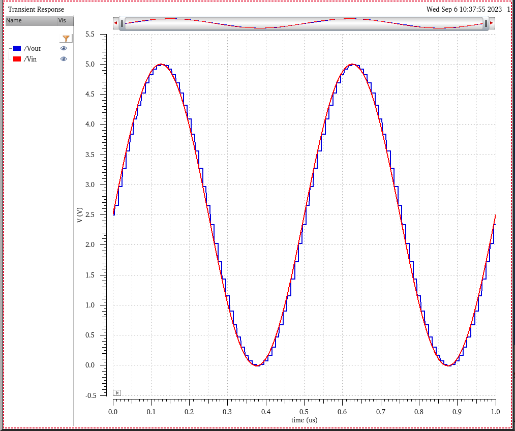
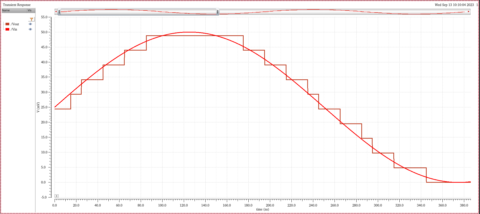
2) Discussion of simulation results (altered to see exaggereated step size)
From the simulations show above we can see that the spacing between each step changes around the input voltage.
The step size is correlated to the LSB or the minimum change in inout to see the change in the output.
3) Determining LSB on ADC input is a relatily simple task as we can use the derived formula
1LSB
= VDD/2^N where N is the number of bits. So if we have VDD = 5V
and a 10bit ADC our LSB should be 4.883mV as seen in the plot above.
Lab Results:
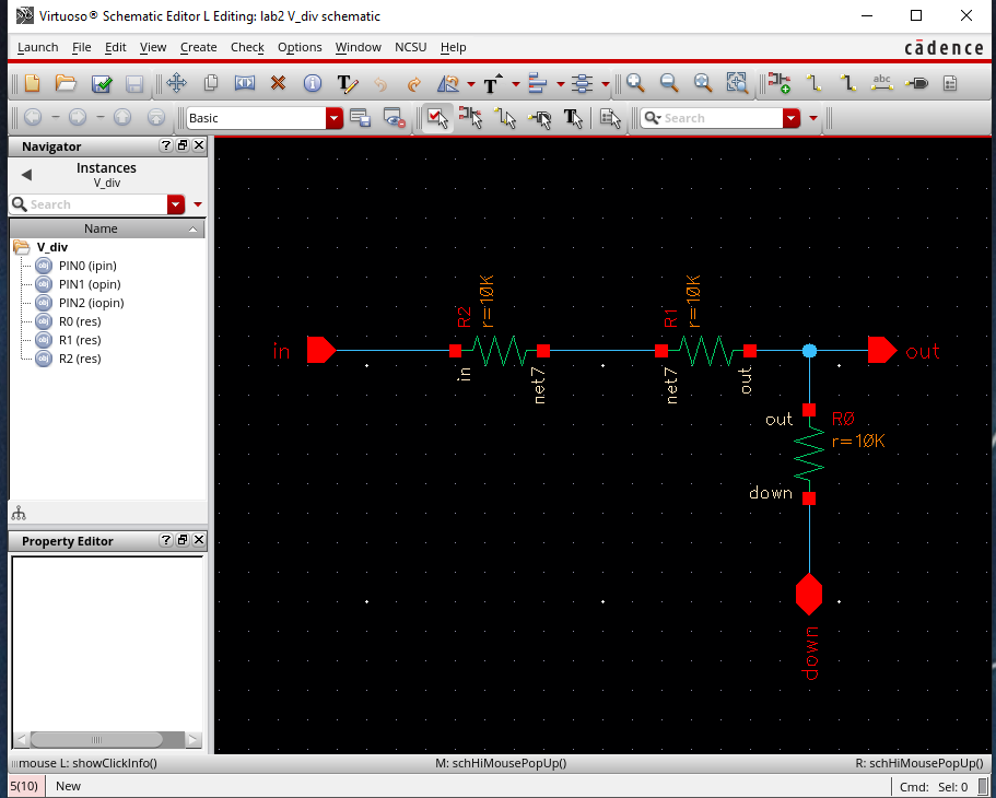
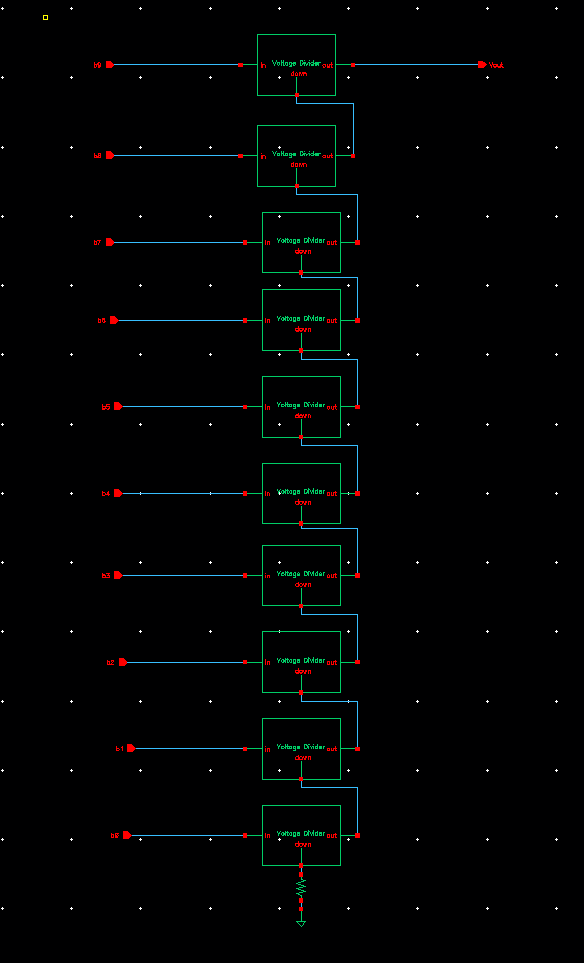
To find the resistance of a 10bit DAC you need to simplify each voltage divider from the bottom
to top using source transformtions and resistor combination rules to find the R_out = R.
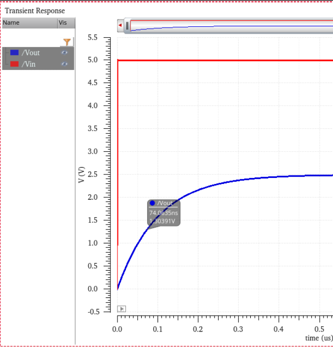
Assuming a 10pF load, our estimated delay can be found by td = 0.7*(10k)*(10p) = 70ns
This backed up by the above sim as it shows 74ns.
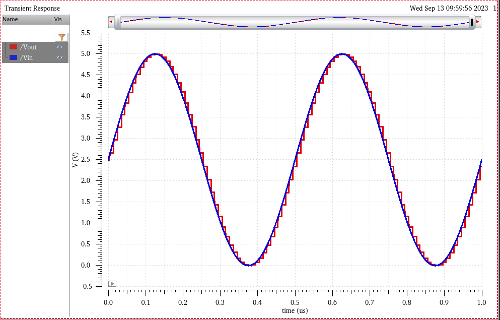
Unloaded DAC to verify operation is identical to provided DAC
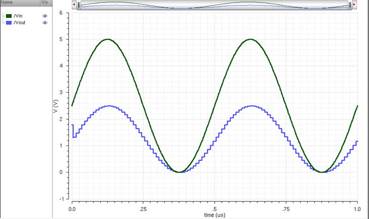
The above shows the DAC with a 10k resistive load.
The resistor creates a voltaeg divider which approximalty halves the voltage
as our output resistance is 10k and our load is 10k.
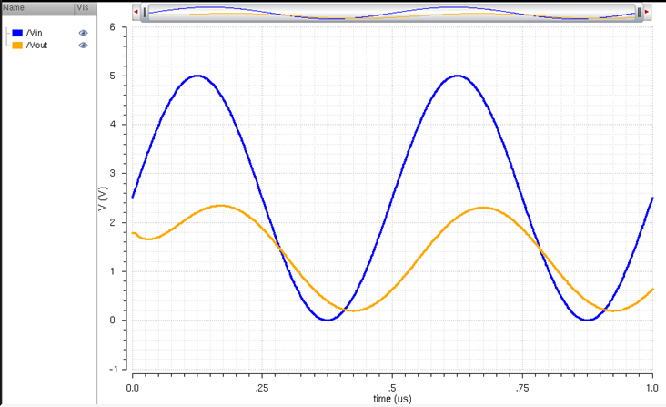
The above shows the DAC with a 10p capacitive load
The capacitor smooths the output but also causes vout to lag the input
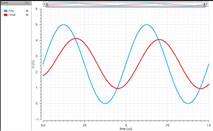
The above shows an R/C load of 10k/10p
The combined load, halves, smooths and introduces lag.
If the switch resisatnce is not small compared to R the R_out would be different
as its resistance is no longer negligible during calacutions.
I tested the convergence fix with the values specified in lab and it worked by forcing the sims using specifc values.I backed up my lab webpage and design directory as shown in last lab