To begin, we created and simulated the schematics and symbols for the
4-bit inverter and 2-to-1 mux/demux.
Lab 7 - ECE 421L
Email: yamame1@unlv.nevada.edu
11/08/23
For this prelab I backed up all of my work, read through the lab and worked through tutorial 5.
Lab Results:
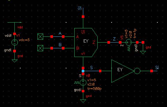
To begin, we created and simulated the schematics and symbols for the
4-bit inverter and 2-to-1 mux/demux.
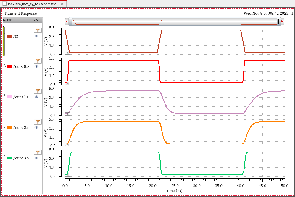
In
our simulation for the inverter we can see how the different capacitive
loads impact the rise/fall times of the output.
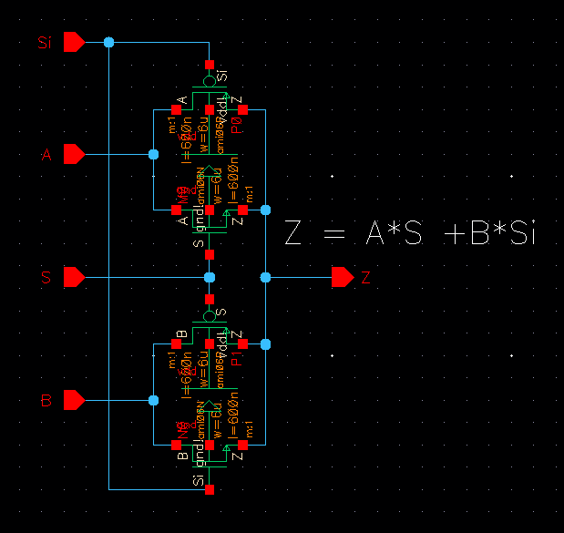
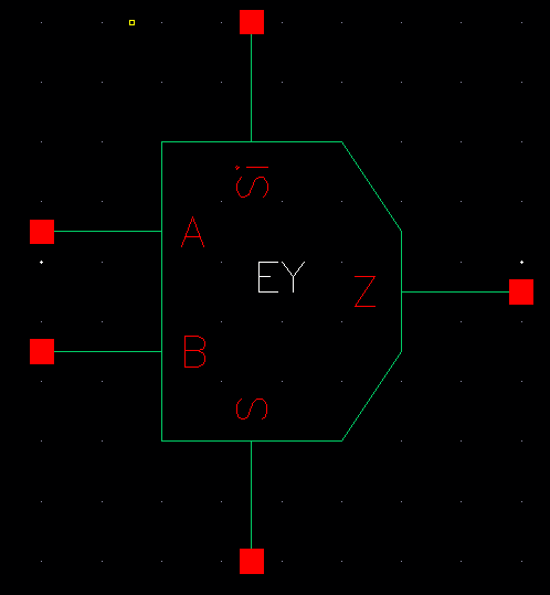
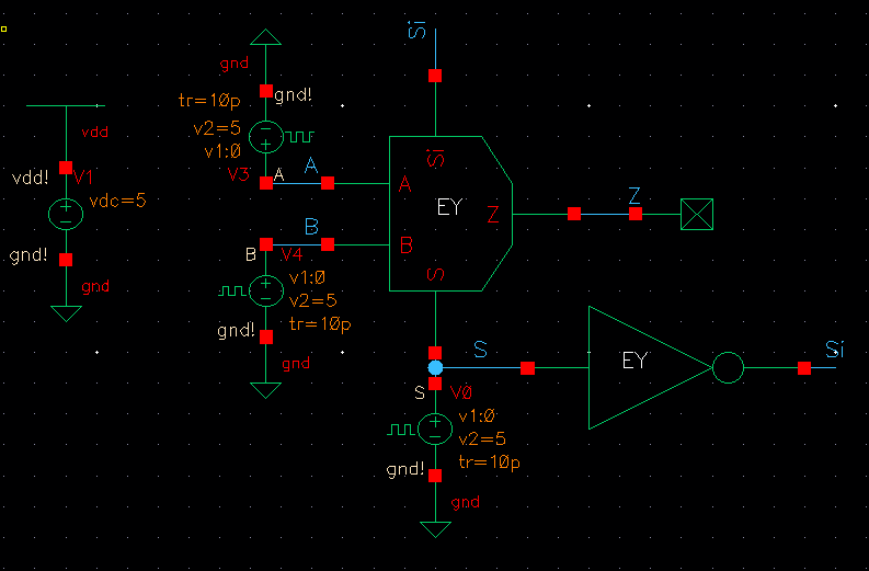
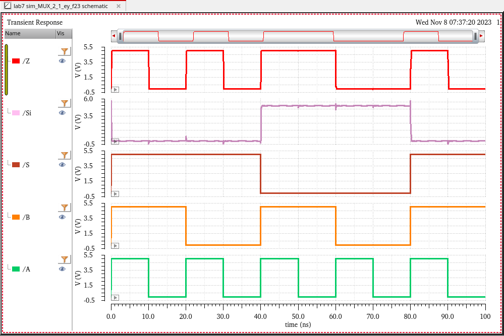
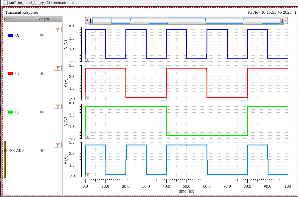
Using the ckt in it's MUX config, we can see that either A or B is passed to Z based on the select input
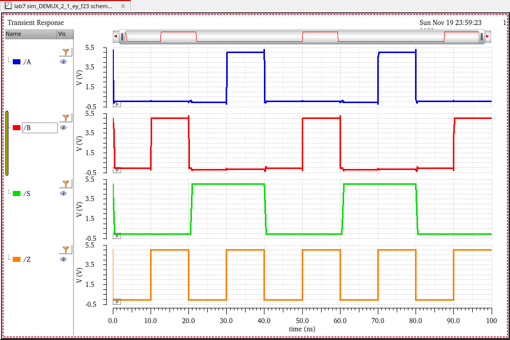
In the DEMUX config. we see that Z is passed to A or B depending on the select input
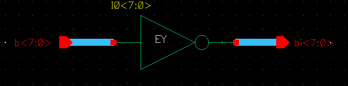
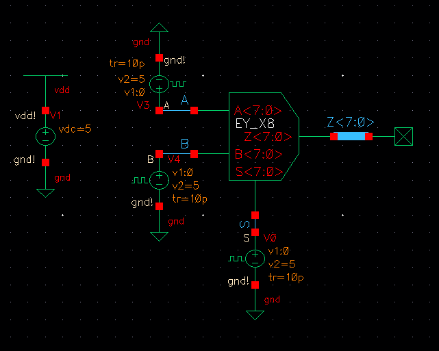
Now we will work with buses and arrays to create the schematic, symbol and simulate
8-bit devices using 1-bit versions of the device.
8-bit INVERTER
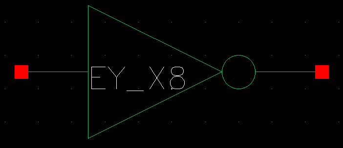
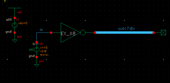
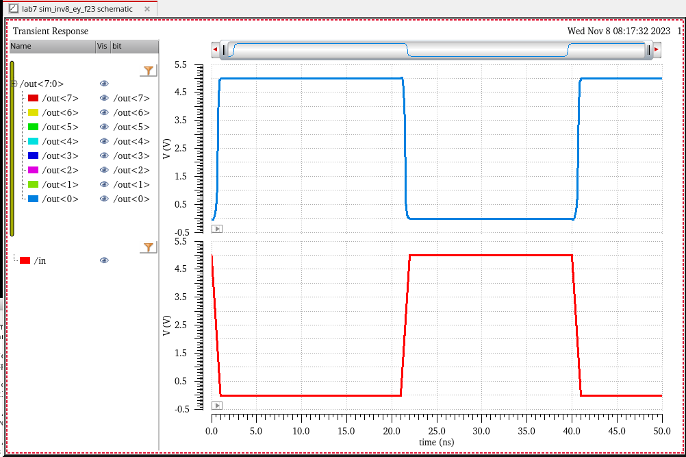
We can see that without the capacitive load in the 4-bit sim, all the inputs and outputs are the same.
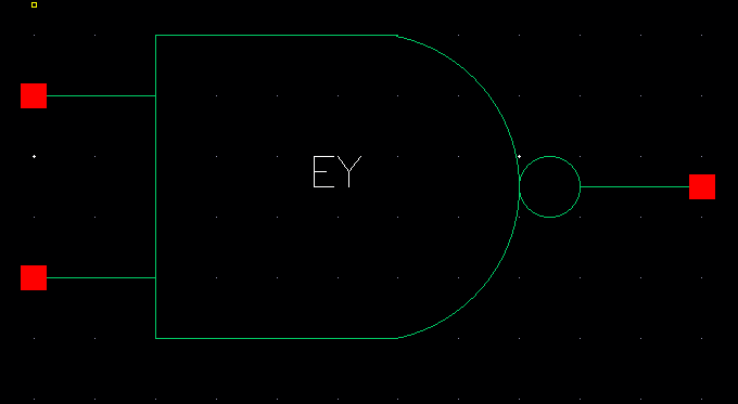
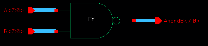
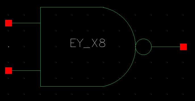
8-bit NAND
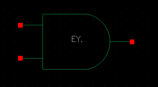
We start by making the 1-bit 2 input NAND gate 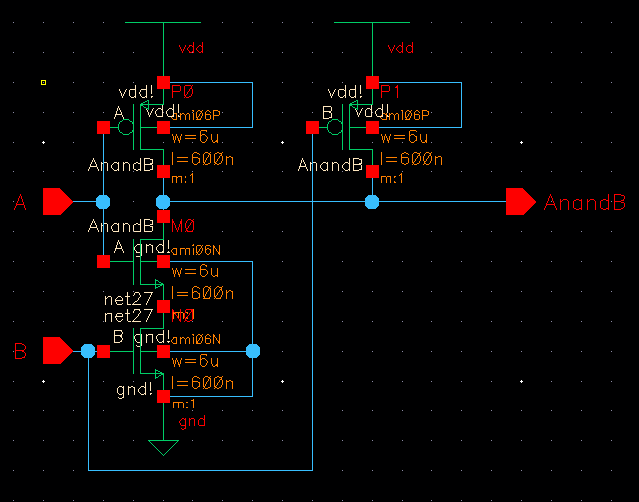
Now we can use arrays of the gate and buses to create an 8-bit version
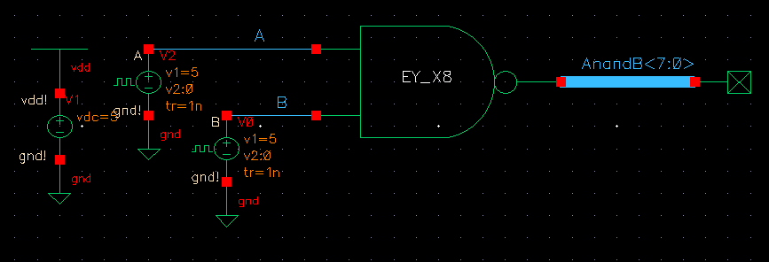
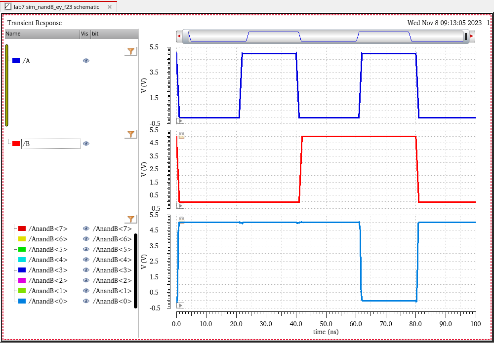
From our sim we can see that the output is only low when box inputs are high, as a NAND should function.
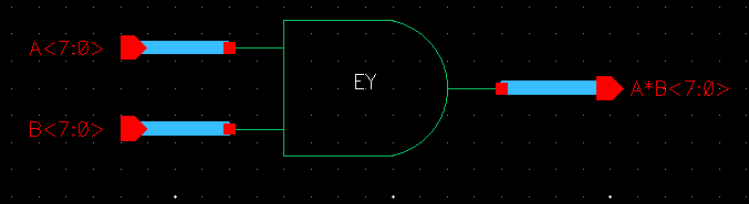
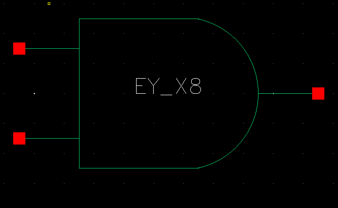
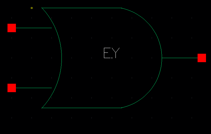
8-bit AND
Like before we begin with making the 1-bit version
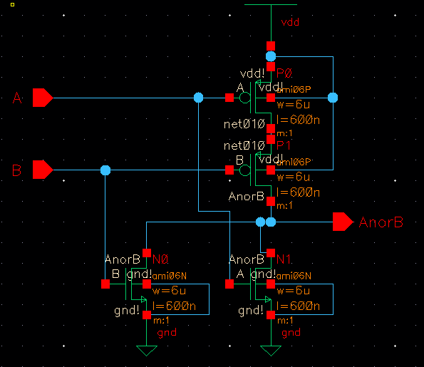
We will use a NOT on the NAND we already made to avoid
making another gate entirely
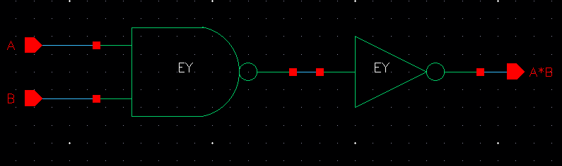
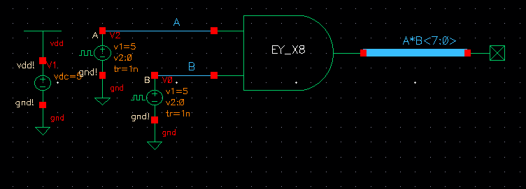
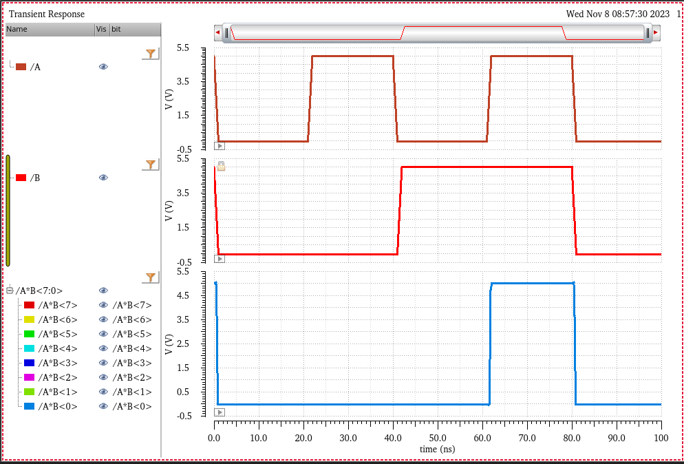
We can see that our AND preforms as expected only being high when both inputs are high.
8-bit NOR
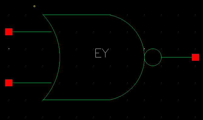
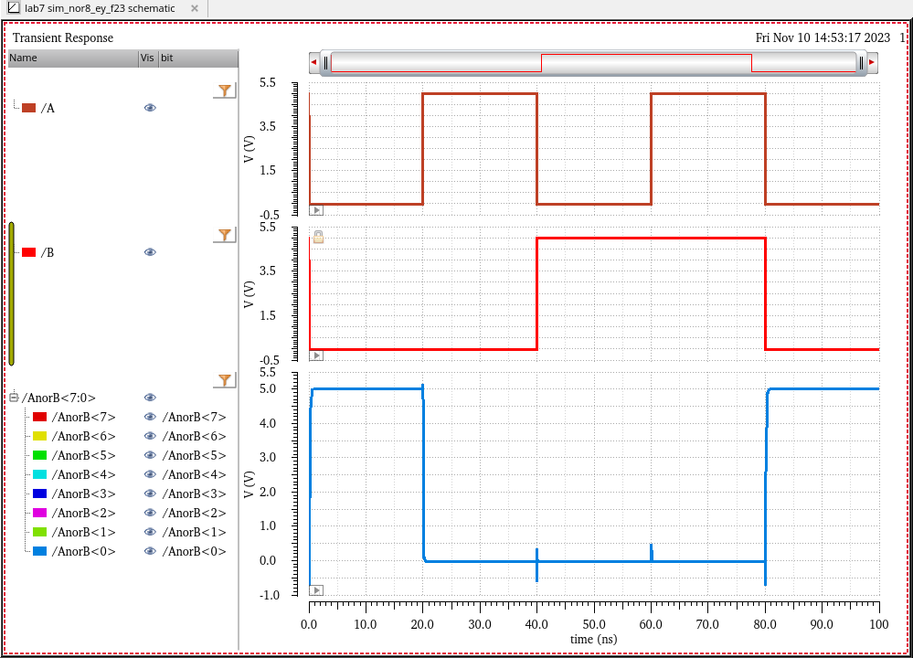
Looking at the sim for the NOR gate we see it is only high when both input are low as expected
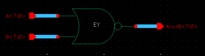
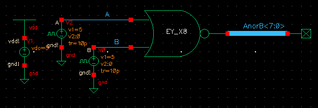
8-bit OR
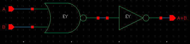
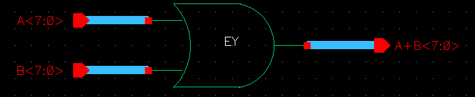
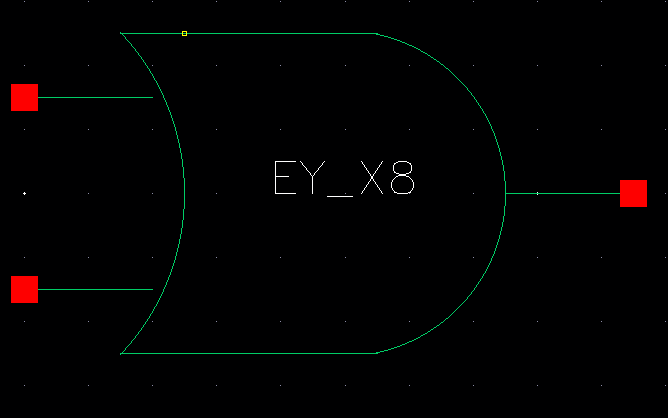
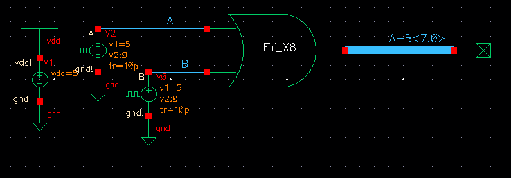
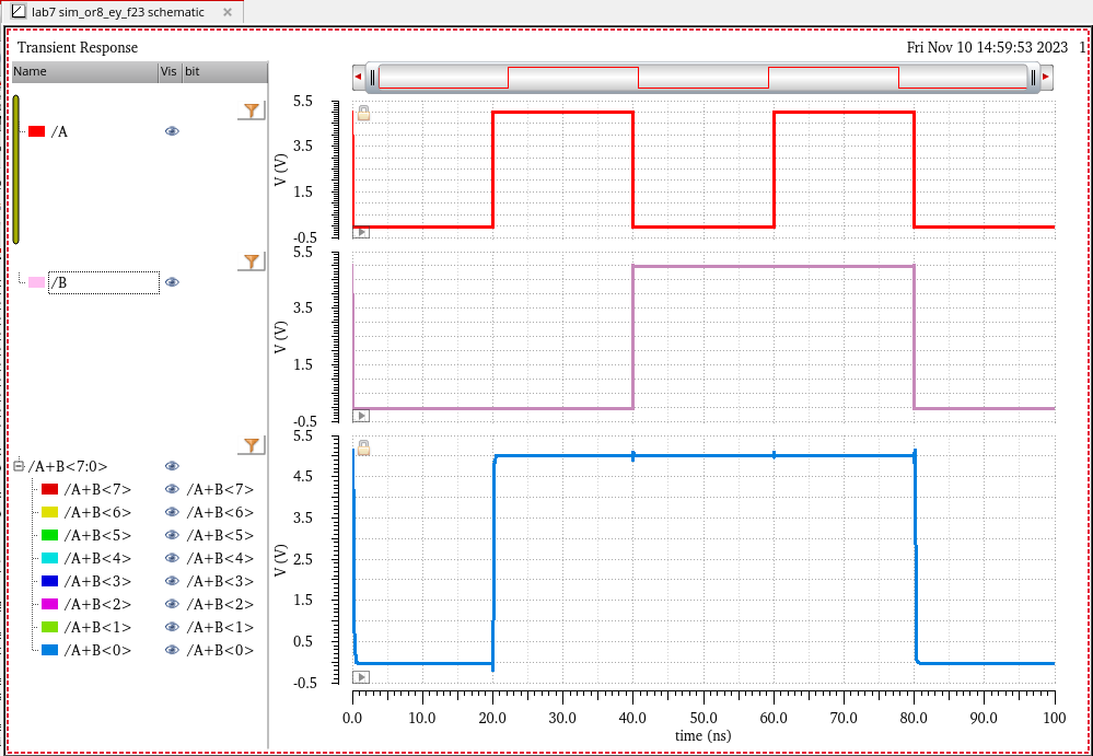
Based on the simulation we can see the OR preformed as expected.
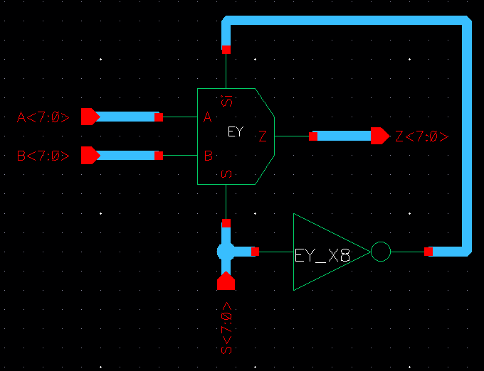
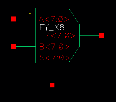
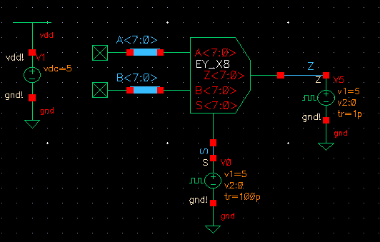
8-bit DEMUX/MUX
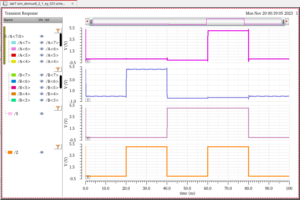
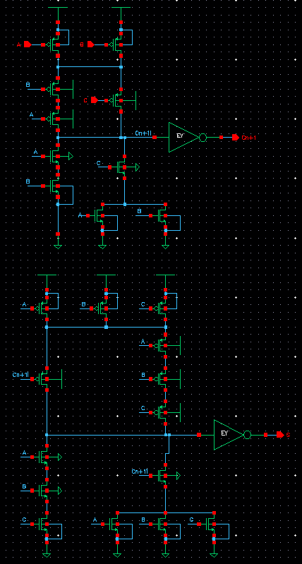
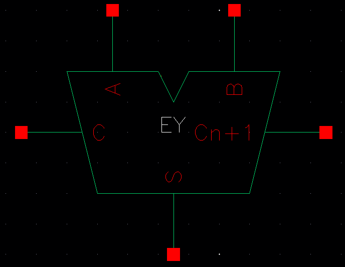
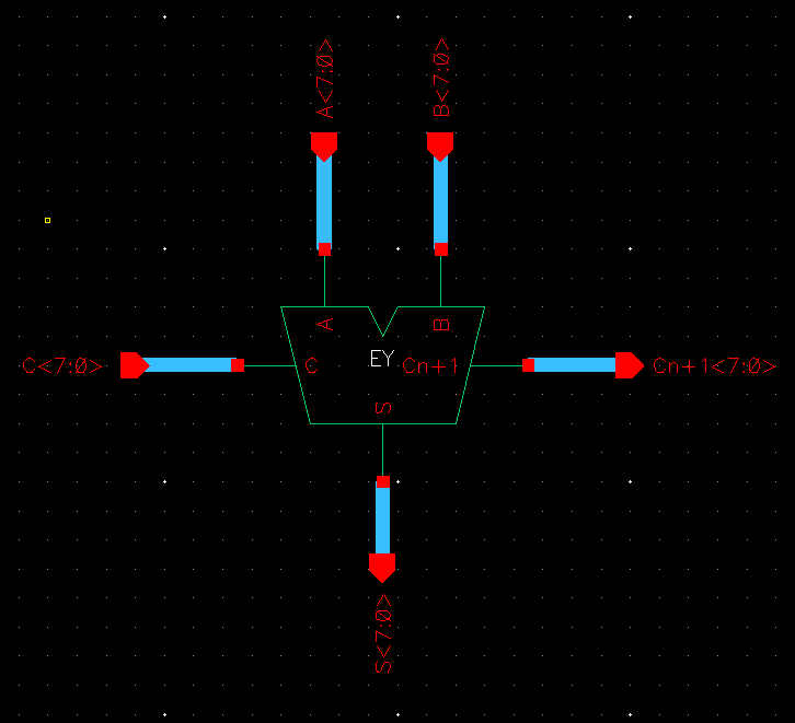
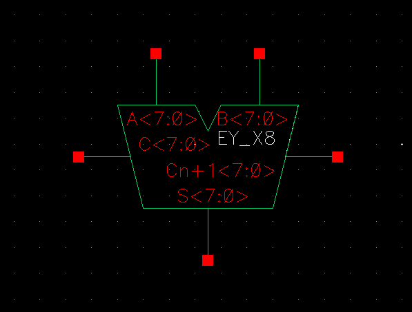
8-bit Full Adder
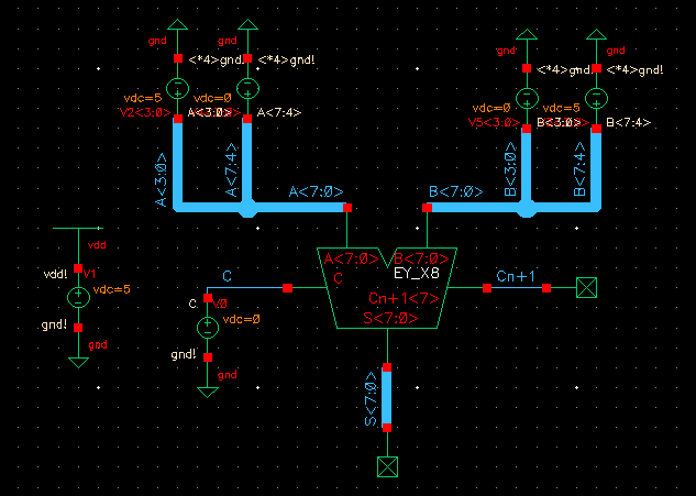
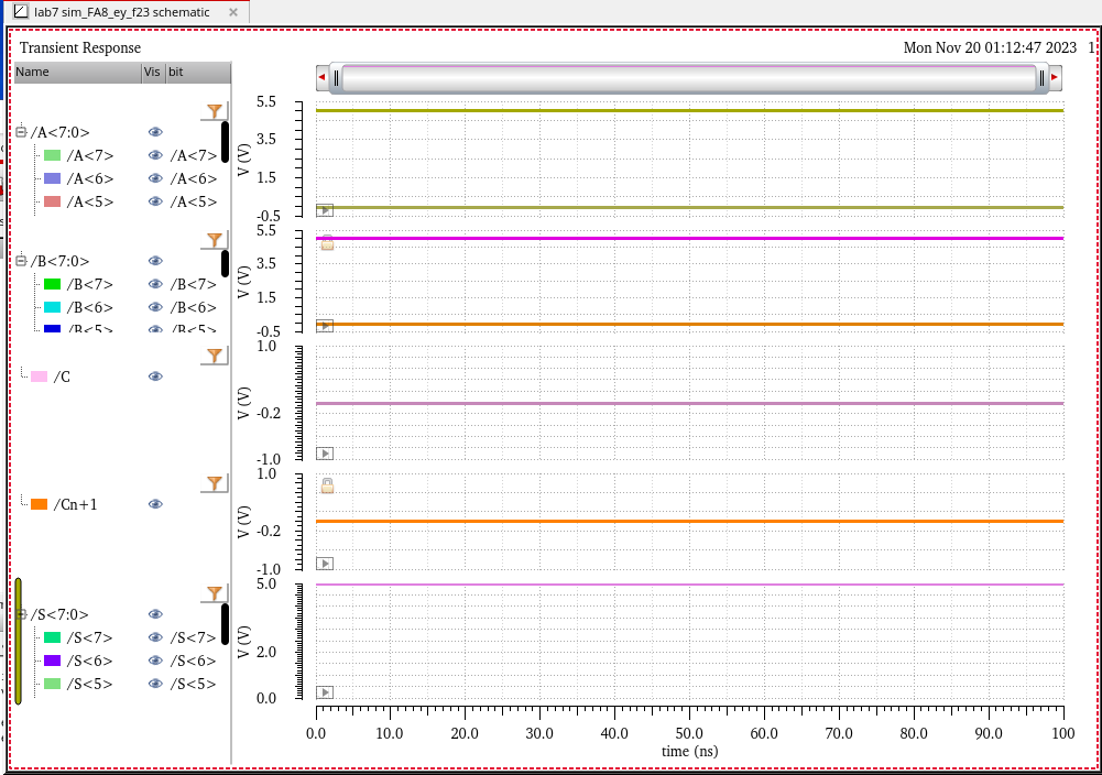
Here we are adding A = 00001111 and B = 11110000 with our carry-in = 0.
This yields an output of S = 11111111 and Carry-out = 0 as demonstrated in the sim below
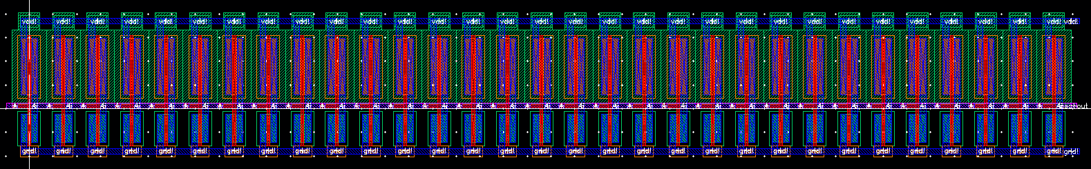
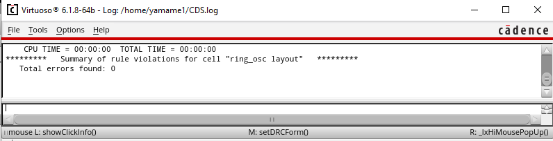
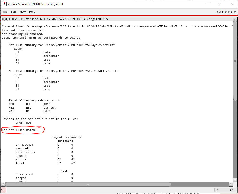
We now know our circuit works so lets lay it out and DRC/LVS
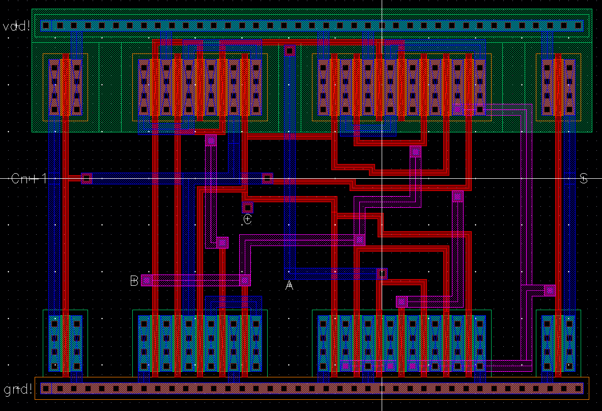
This is the layout of a single full adder. We will now string these togeather into an 8-bit adder
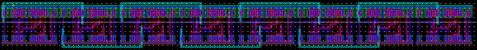
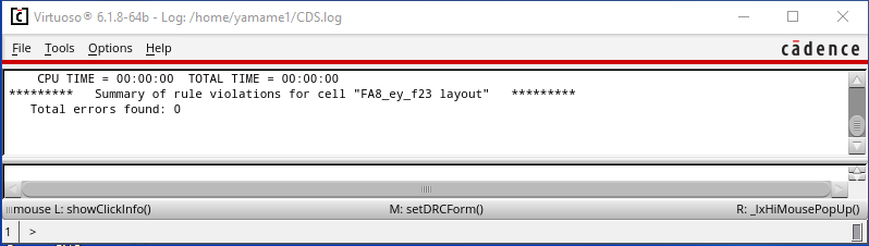
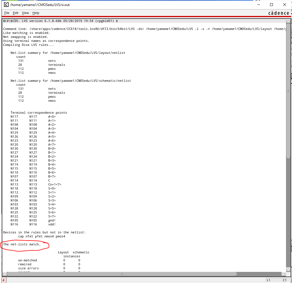
As we can see our 8-bit FA layout returns a clean DRC and LVS.