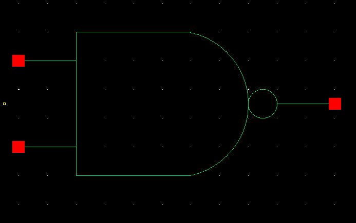
Schematic Symbol
Lab 6 - ECE 421L
Email: yamame1@unlv.nevada.edu
10/25/23
Prior to lab I back up all of my work and went through tutorial 4.
Below I posted pictures of my NAND gate
Schematic
Symbol
Here is the layout as tutorial 4 instructed with the device sizes adjusted to match schematic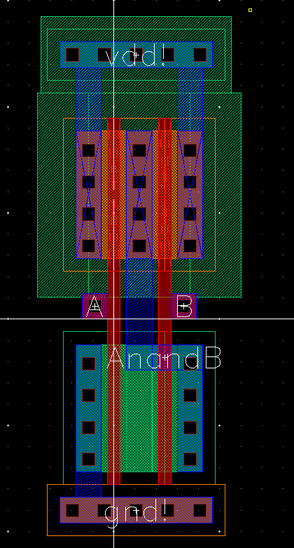
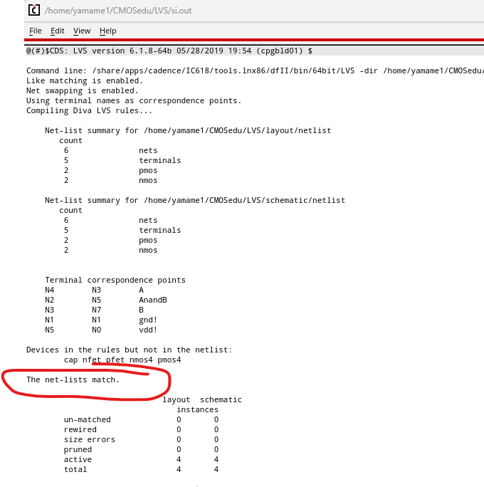
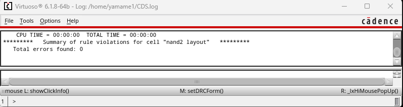
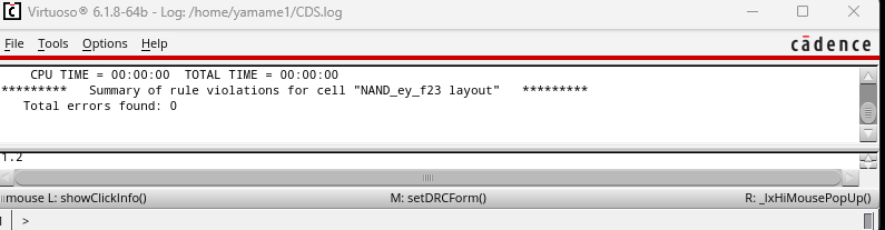
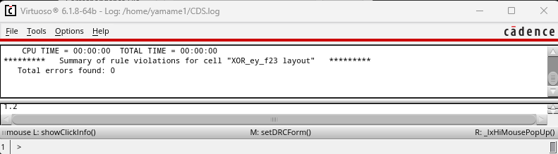
Above I included the DRC and LVS of my layout
Lab Results:
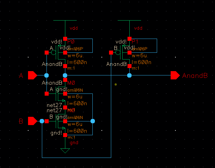
NAND GATE:
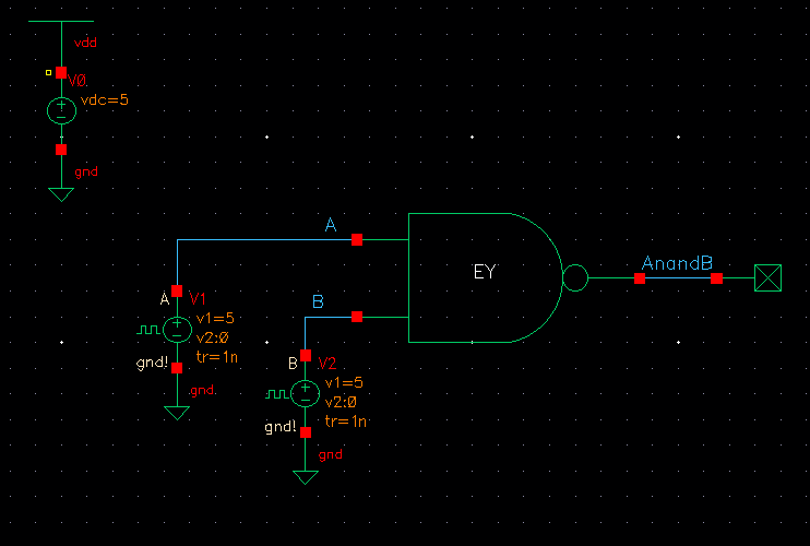
Similar to the prelab we made a layout and symbol for a NAND 2 using 6u/0.6u NMOS and PMOS
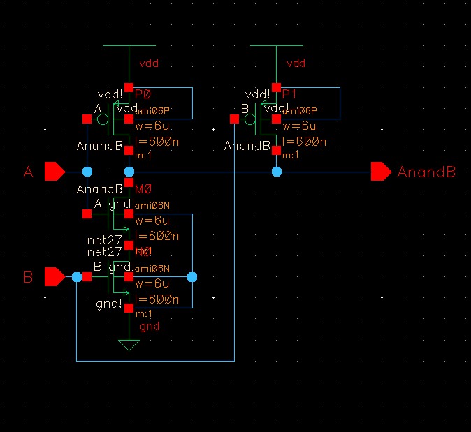
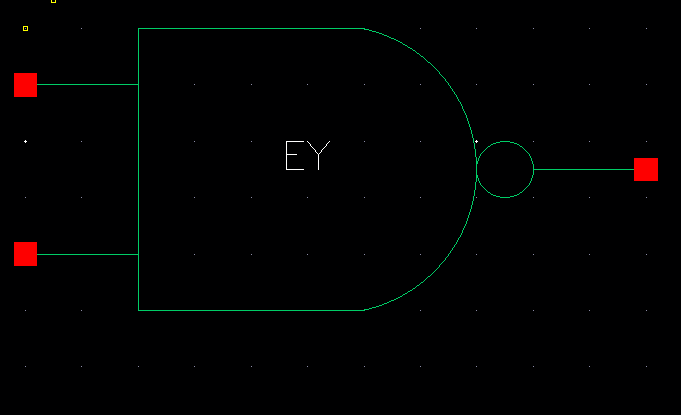
Schematic Symbol
Again like the prelab this is the layout, DRC and LVS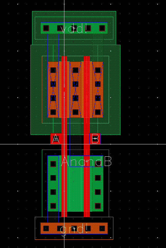
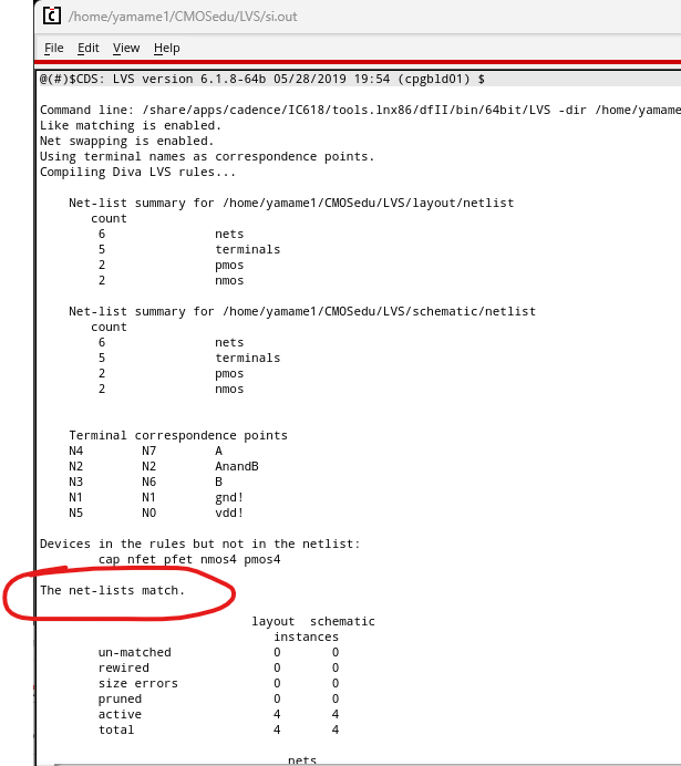
Once we verified our layout was good, we simed our NAND gate to verify its operation for two inputs
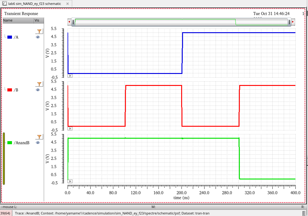
| A | B | AnandB |
| 0 | 0 | 1 |
| 0 | 1 | 1 |
| 1 | 0 | 1 |
| 1 | 1 | 0 |
As we can see from the NAND truth table, our simulation matches
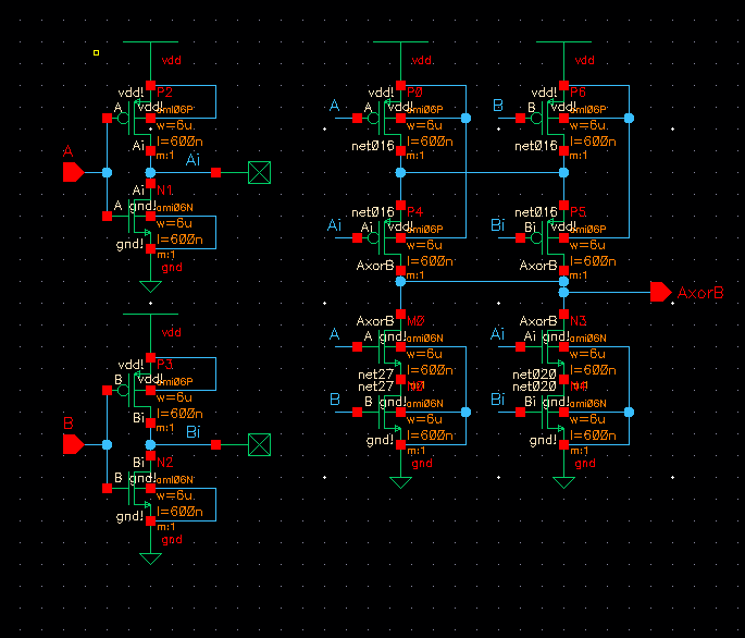
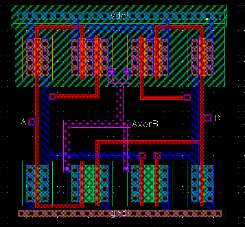
XOR GATE:
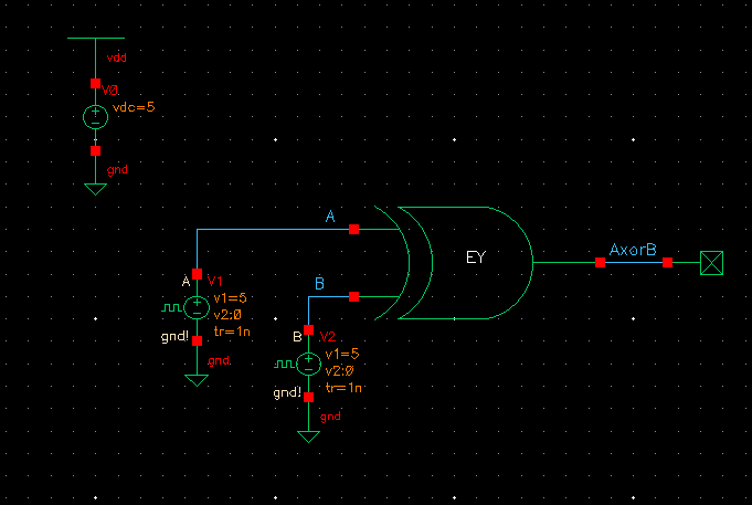
For this part we made a two input XOR gate using 6u/0.6u NMOS and PMOS
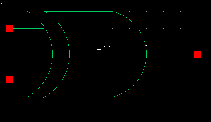
Schematic Symbol
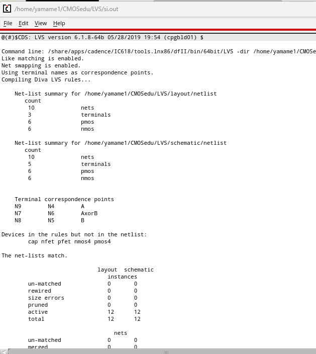
Now, here is my layout with DRC/LVS both are clean.
We can now sim to verify that our XOR gate works as expected for two inputs
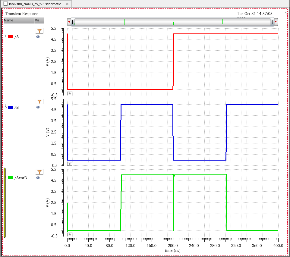
A small note here. We can see the output dip during the transition from the 01 -> 10
This "glitch" occurs as a fucntion of the rise/fall times of the inputs.
The times where the transitors are switching when the input is between VIL and VIH
aka "no man's land", results in a contention current where the transitors are
trying to pull the output high and low at the same time. This is why its important
to have fast clock edges so that the transistors arent on very often so that you
have less charge pull. Slow edges that cause the transitors to be on for a long time
(relative) can result in heating issues eventually resulting in failure of the chip.
Input and output buffers help to mitigate this issue by squaring up the inputs
ie decreasing the rise/fall times so that all the signals on chip have fast edges.
I decided to leave it with these rise/fall times to exagerate the effect
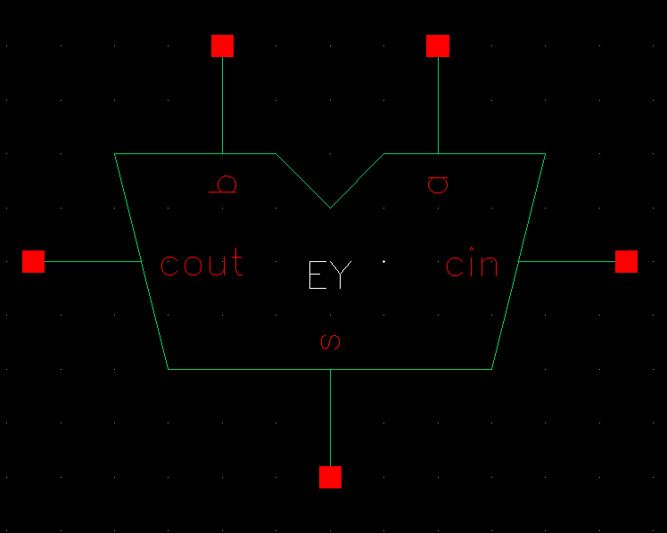
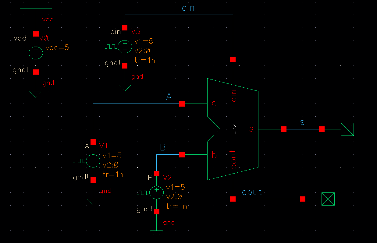
Full Adder:
Now we can combine the NANDs and XORs to create a full adder (FA).
Again we will start with the schematic and symbol for our FA.
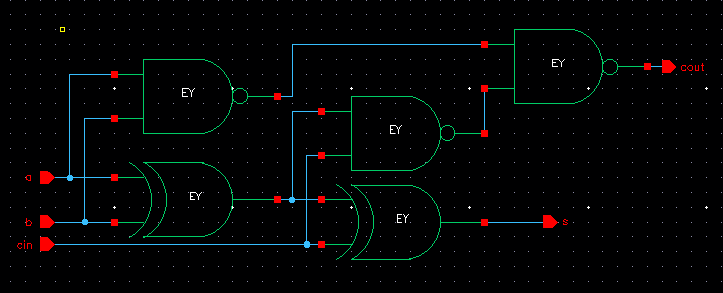
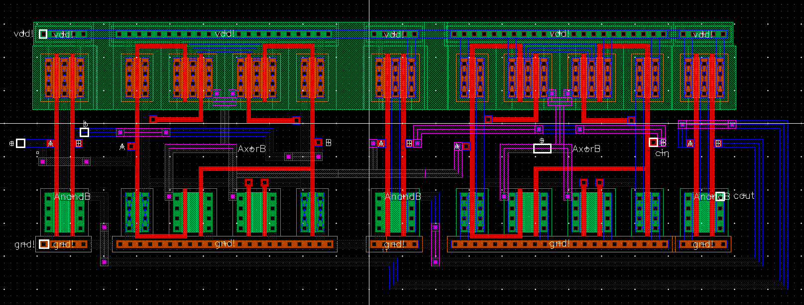
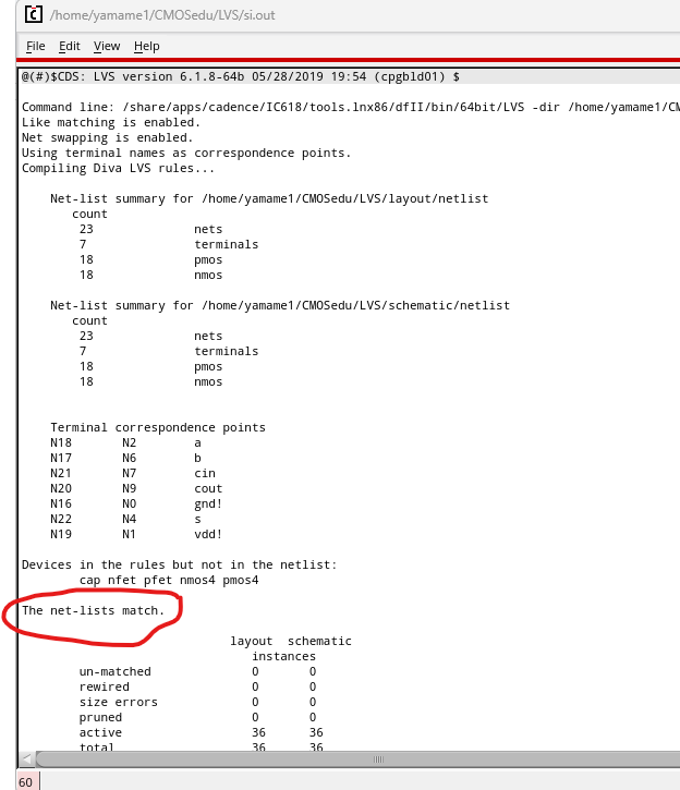
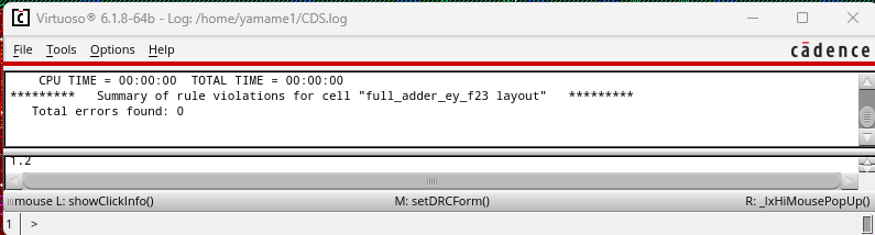
Now for the fun part. This is the layout with clean DRC/LVS. It could certainly be cleaner but this works.
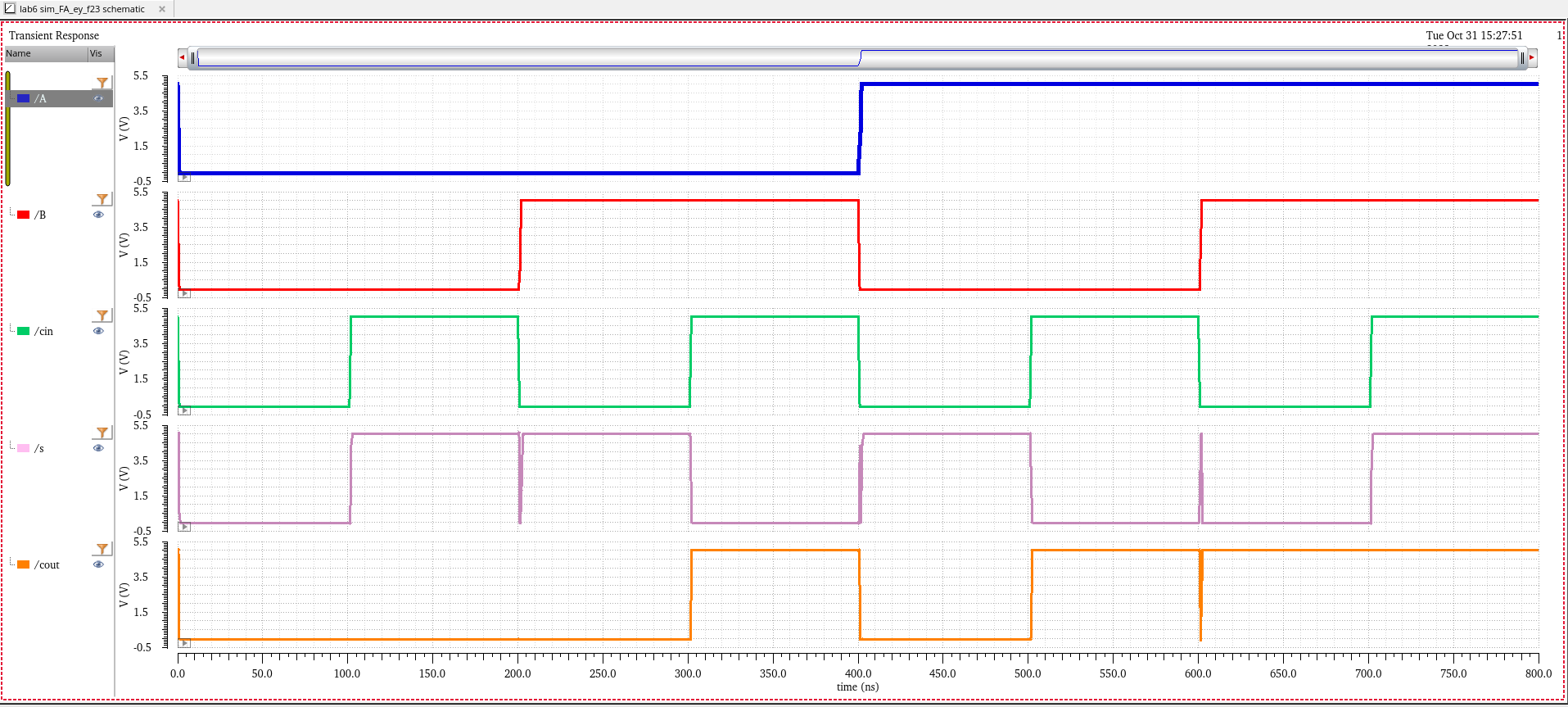
a | b | cin | s | cout | |
0 | 0 | 0 | 0 | 0 | |
0 | 0 | 1 | 1 | 0 | |
0 | 1 | 0 | 1 | 0 | |
0 | 1 | 1 | 0 | 1 | |
1 | 0 | 0 | 1 | 0 | |
1 | 0 | 1 | 0 | 1 | |
1 | 1 | 0 | 0 | 1 | |
1 | 1 | 1 | 1 | 1 |