Lab 5 - ECE 421L
Authored
by Ethan Yamamoto,
Email: yamame1@unlv.nevada.edu
10/8/23
Lab Description:
Design, layout, and simulation of a CMOS inverter
Prelab Description:
Prior to lab I back up all of my work and went through tutorial 3.
Below I posted pictures of my inverter schematic, layout, symbol, DRC and LVS as instructed my Tutorial 3.
Lab Results:
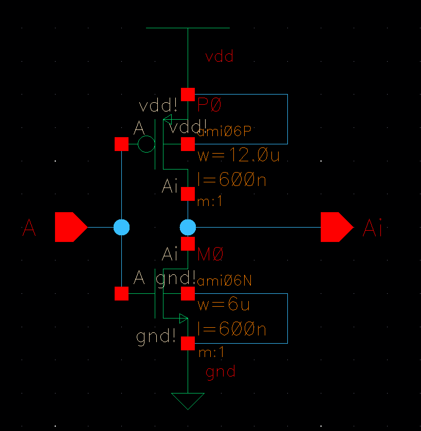
12u/6u:
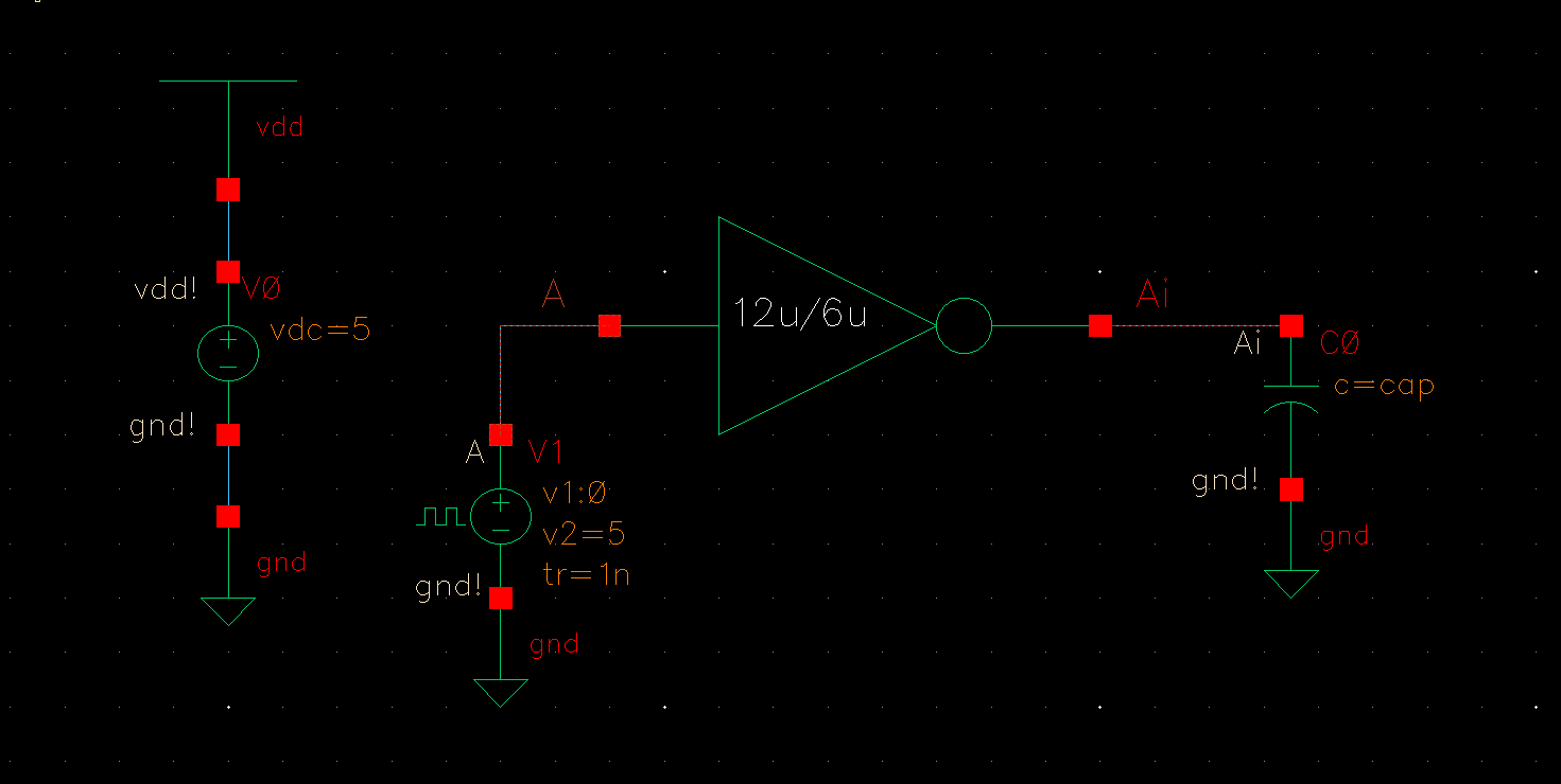
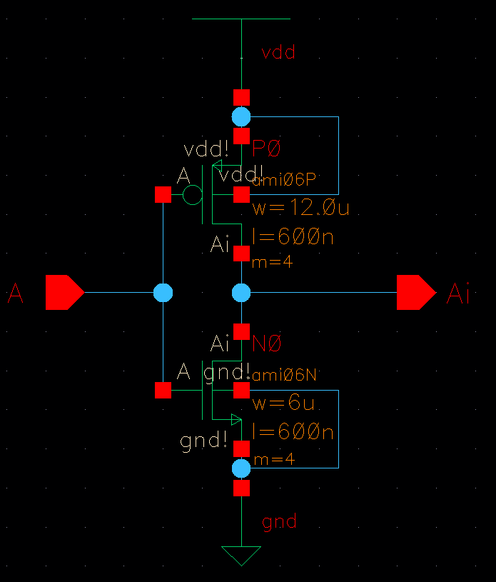
Starting off this lab I made a 12u/6u inverter. I posted the schematic below
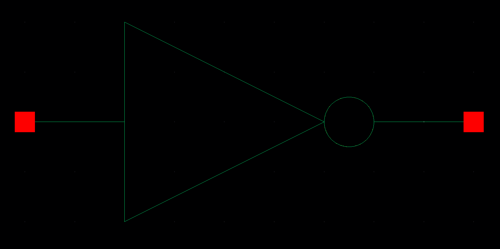
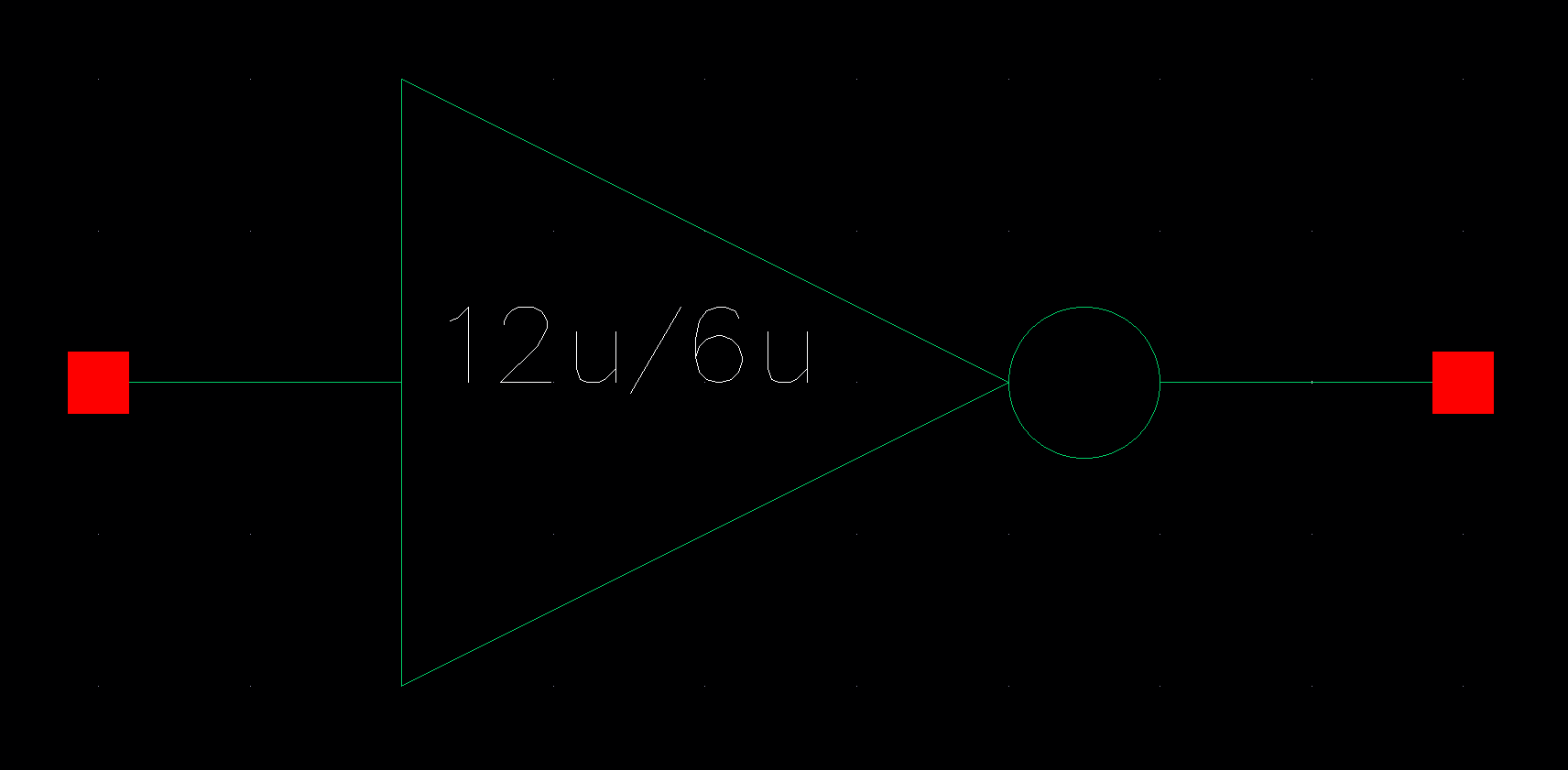
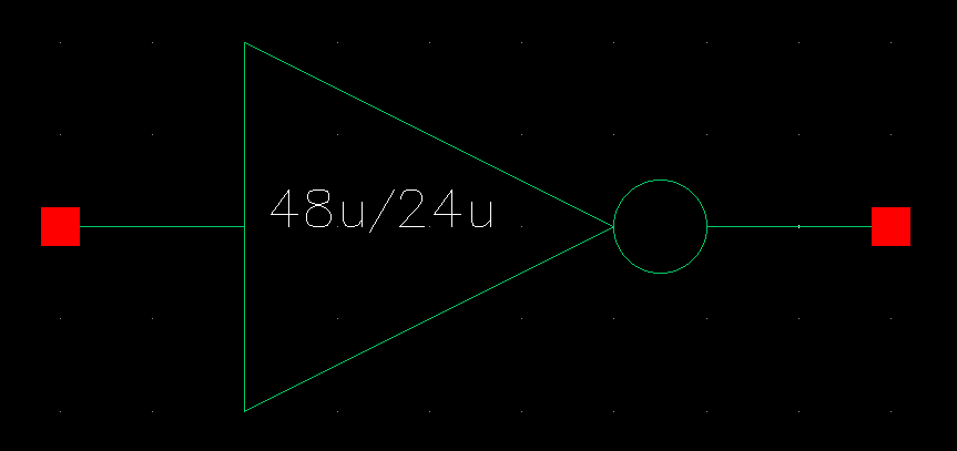
This is the symbol of the 12u/6u
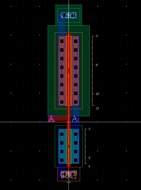
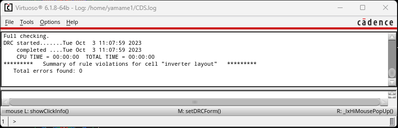
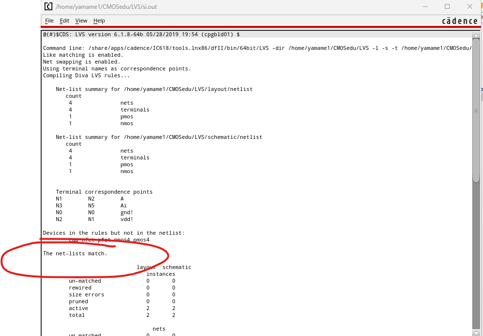
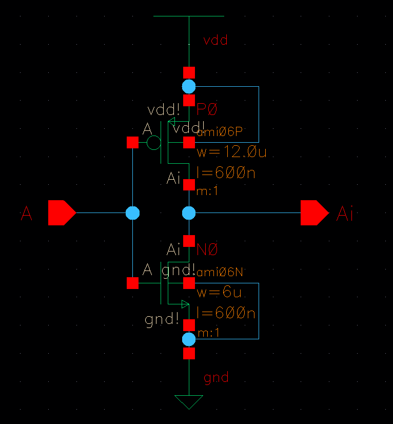
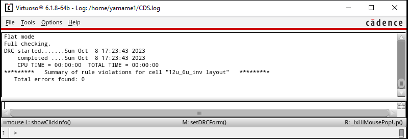
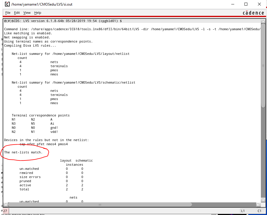
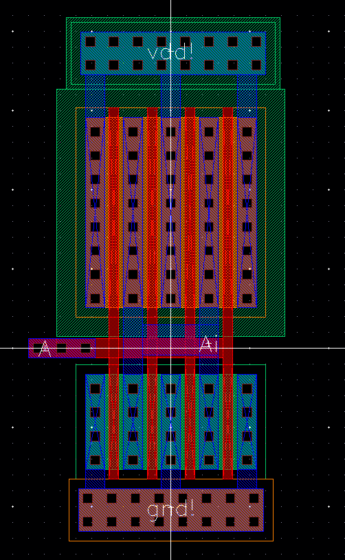
Here is the layout, DRC and LVS of the 12u/6u
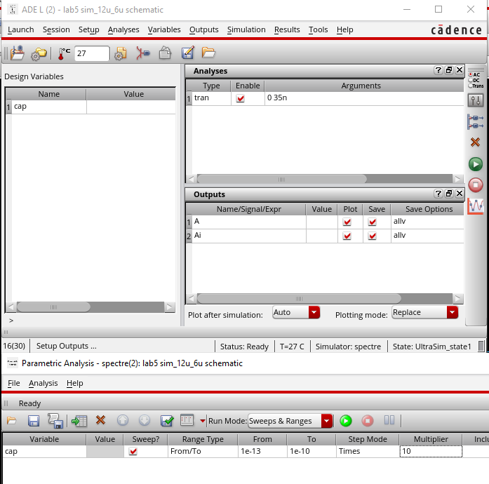
This is the simuation schematic and setup
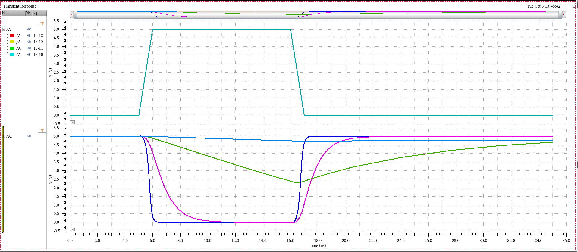
This the Ultrasim result for 100 fF, 1pF, 10pF, and 100pF capacitive load on the 12u/6u
This is the ADE L result for 100 fF, 1pF, 10pF, and 100pF capacitive load on the 12u/6u
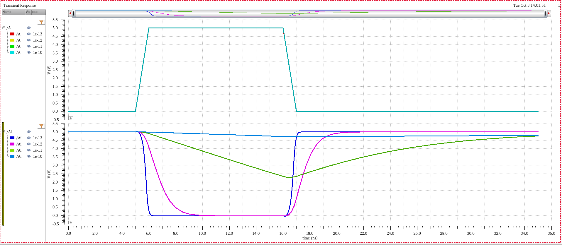
In both we can see that the larger capacitance takes longer to equailize as expected.
The results between Ultrasim and Spectre do differ slightly and ultrasim took much longer to run
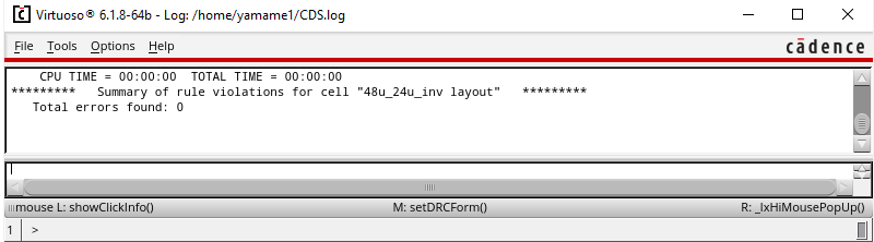
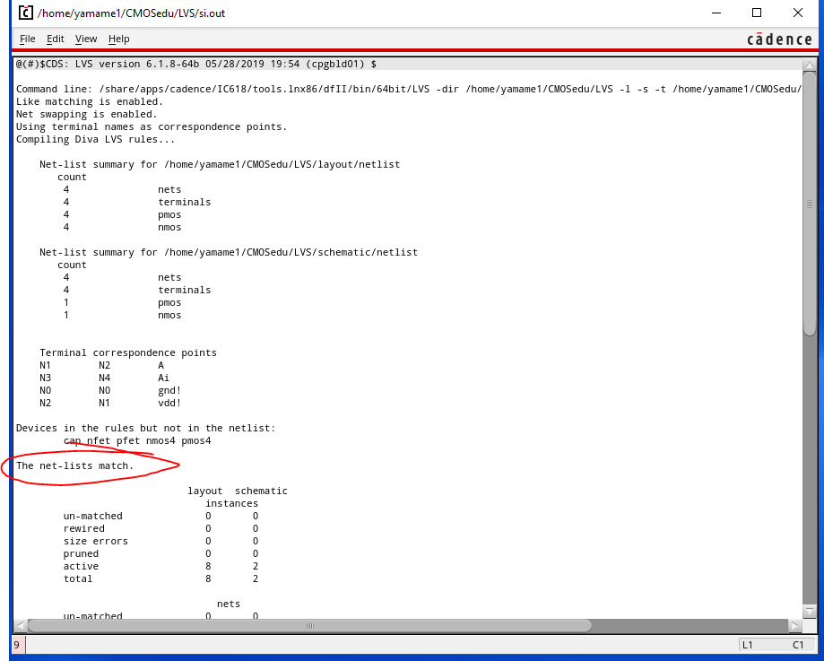
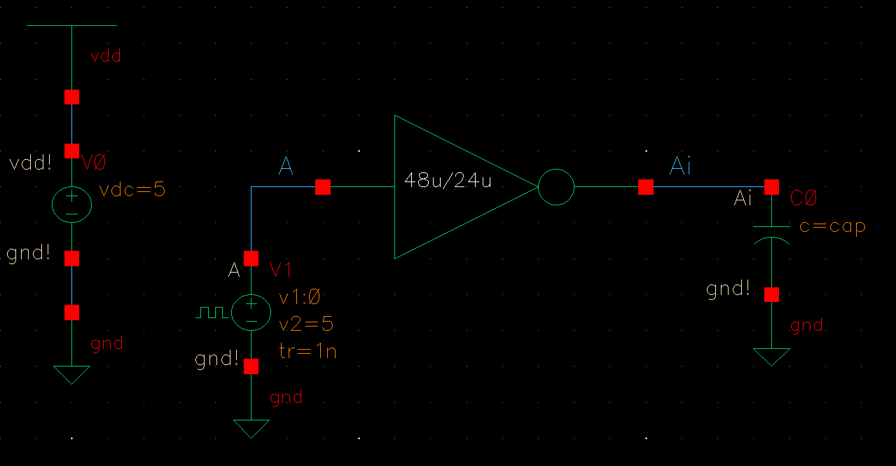
48u/24u
Here is my schematic and symbol for my 48u/24u inverter
This is the layout, DRC and LVS of the 48u/24u
Next I did the simulation as shown below.
Starting with a picture of the schematic, setup then the ADE L followed by Ultrasim
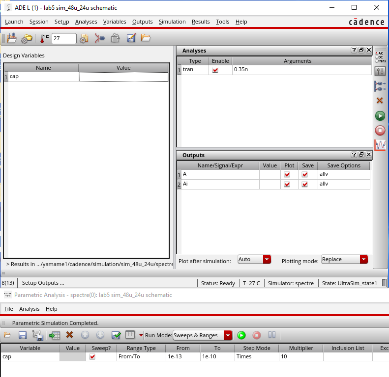
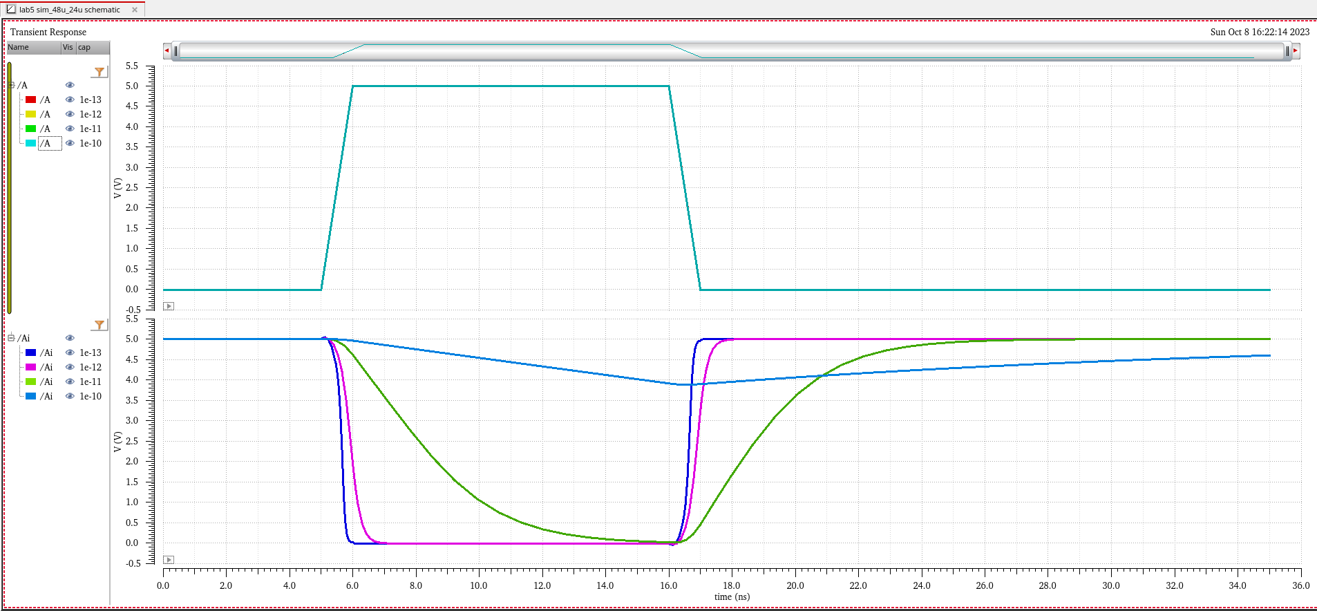
This the ADE L (spectre) result for 100 fF, 1pF, 10pF, and 100pF capacitive load on the 48u/24u
This the Ultrasim result for 100 fF, 1pF, 10pF, and 100pF capacitive load on the 48u/24u
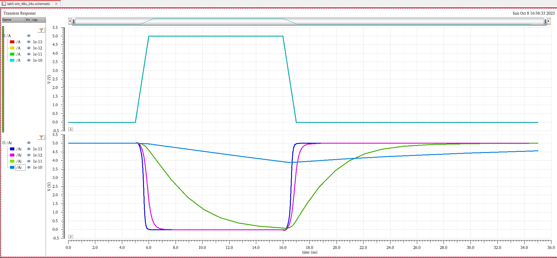
From the sims we can see that the simulations are more "rounded" than the 12u/6u inverter. Id assume this is a result of
an increased parasitic capacitance. Like before we do see some variation between the two tools.
But by and large the simulations show a similar result.
As always I backed up my work.

Ive also zipped the lab files for this lab and linked them here.
Return to EE 421L Labs