Lab 4 - ECE 421L
Authored
by Ethan Yamamoto,
Email: yamame1@unlv.nevada.edu
9/26/23
Lab Description:
IV characteristics and layout of NMOS and PMOS devices in ON's C5 process
Prelab Description:
Prior to lab, I backed up my work as shown below.
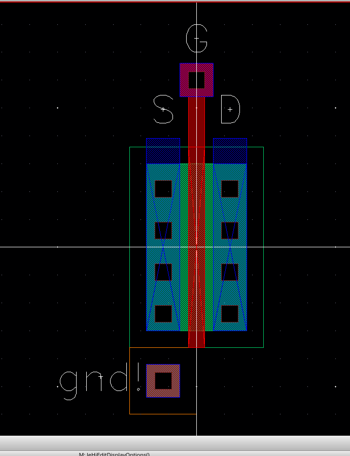
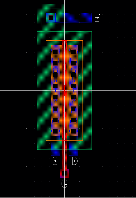
I also read through the lab and completed Tutorial 2. Ive provided
pictures of the NMOS and PMOS layouts below.
Lab Results:
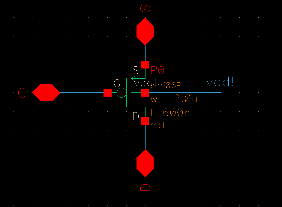
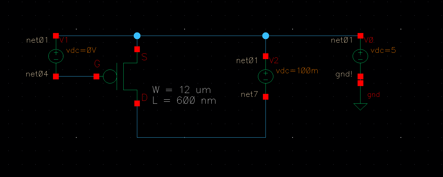
I started by modifying my PMOS by removing the Body pin and instead tying it directly to Vdd.
This involved changing the schematic, symbol, and layout then extracting and prefroming an LVS
resulting in the schematic below.This modification was unessisary on the NMOS as its bulk is
already tied to ground.
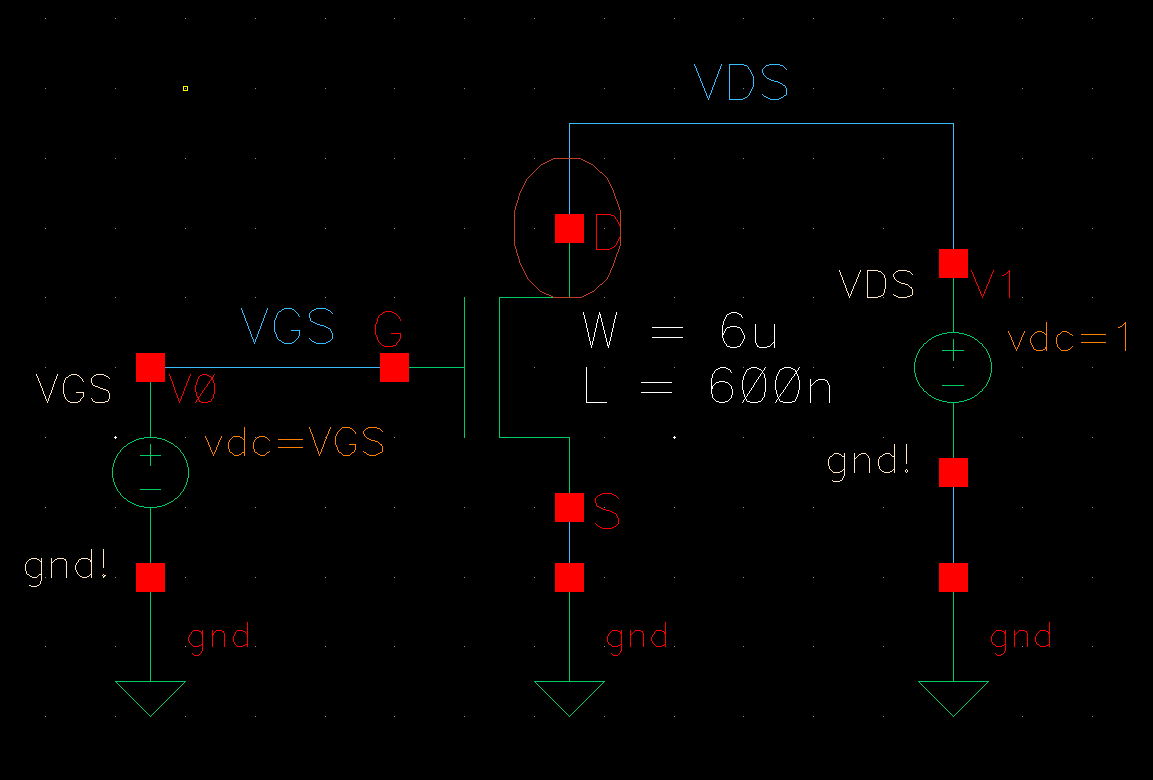
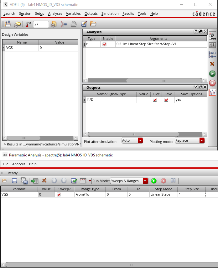
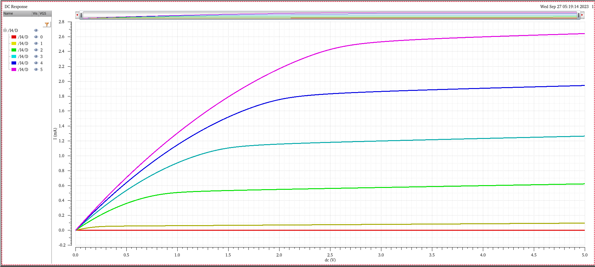
Next I simulated ID v. VDS of an NMOS for VGS varying from 0 to 5 V in 1 V steps while VDS varies from 0 to 5 V in 1 mV steps using a 6u/600n
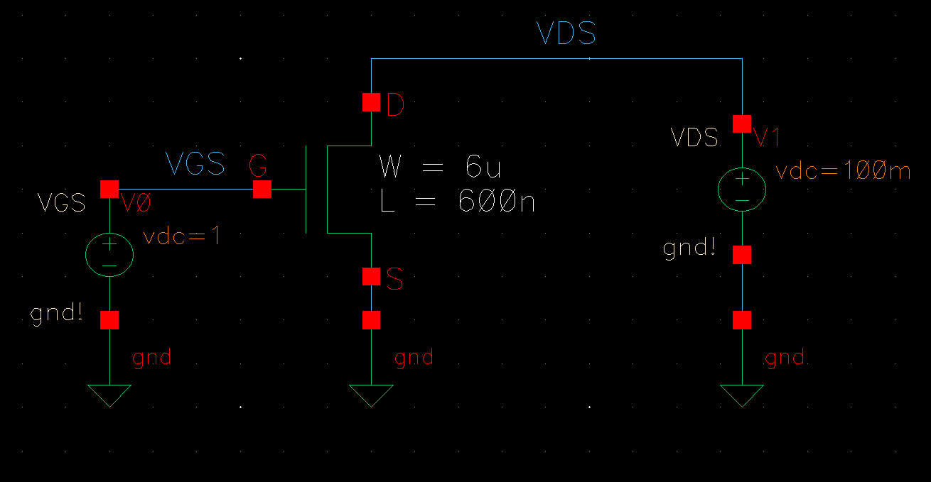
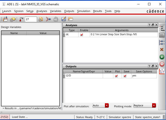
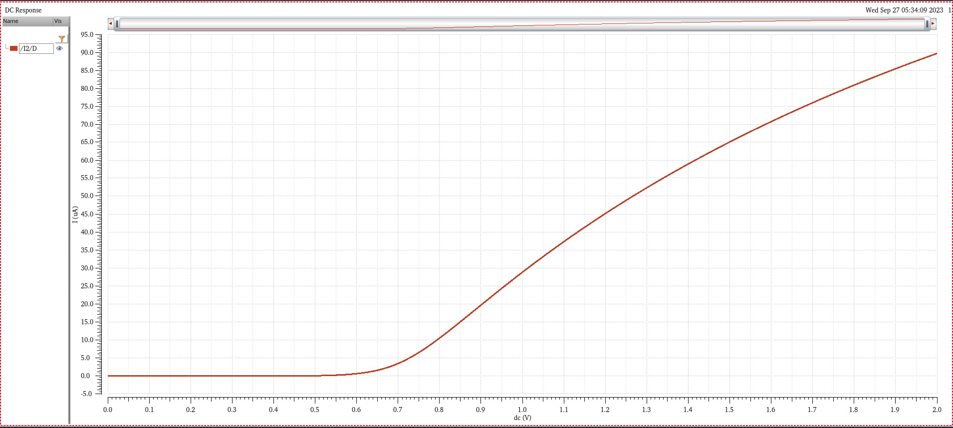
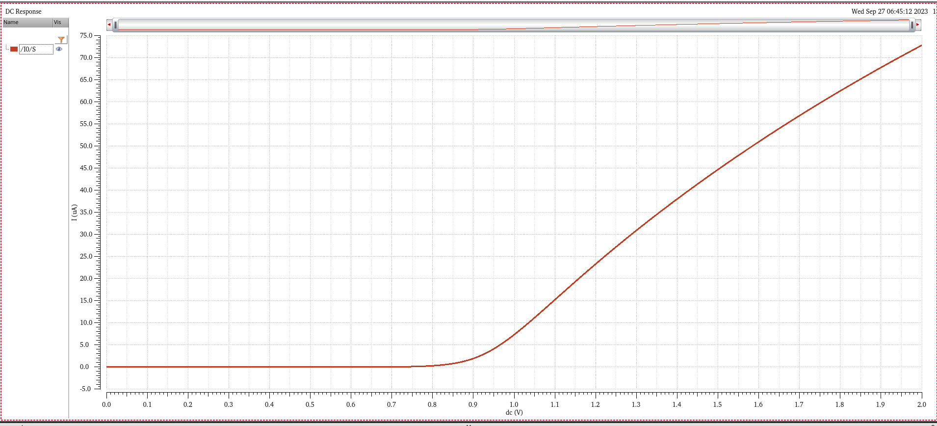
Next I simulated ID v. VGS of an NMOS device for VDS = 100 mV where VGS varies from 0 to 2 V in 1 mV steps using 6u/600n
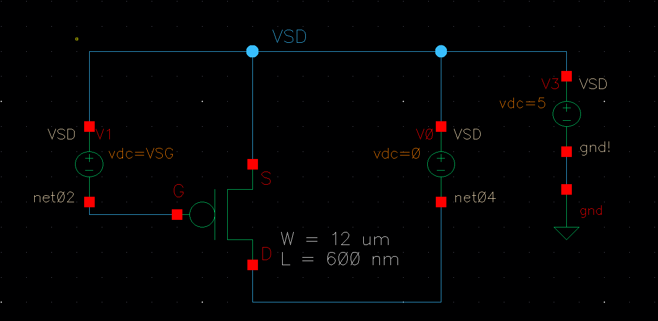
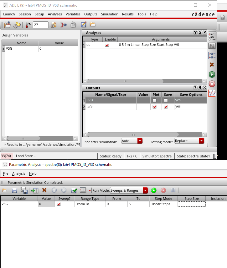
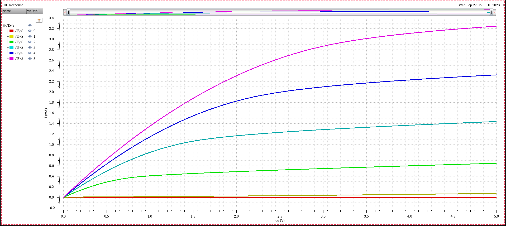
The following job was to simualte ID v. VSD (note VSD not VDS) of a PMOS device for VSG (not VGS) varying from 0 to 5 V in 1 V steps while VSD varies
from 0 to 5 V in 1 mV steps using 12u/600n
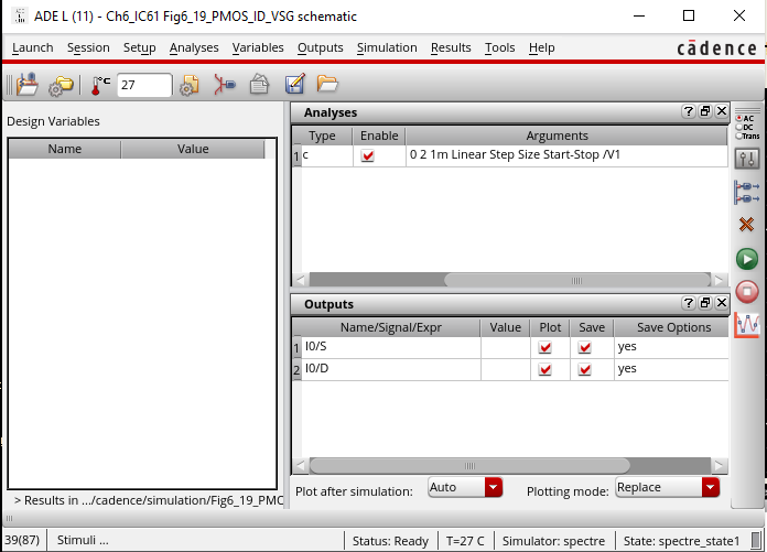
Finally, I simulated ID v. VSG of a PMOS device for VSD = 100 mV where VSG varies from 0 to 2 V in 1 mV steps again using a
12u/600n
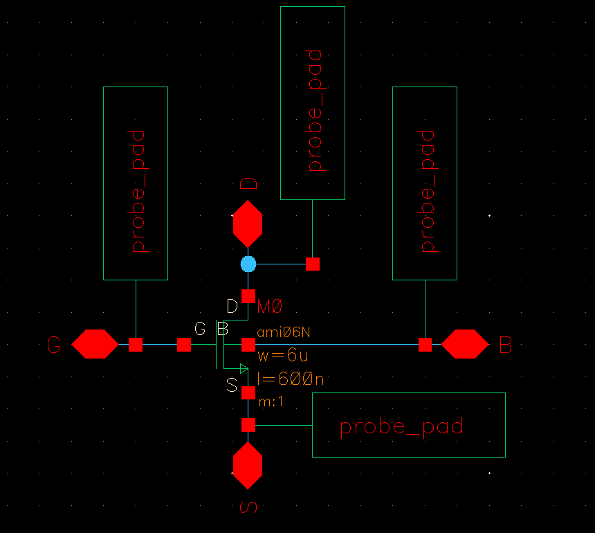
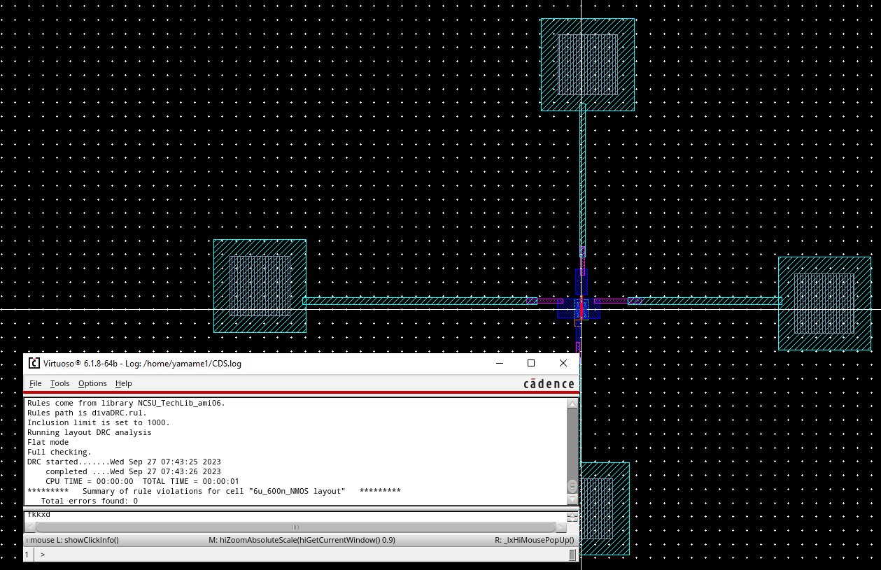
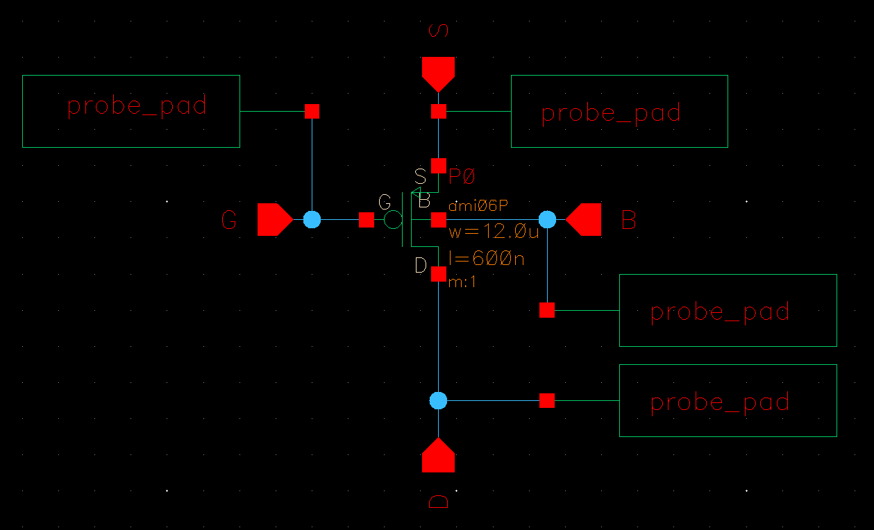
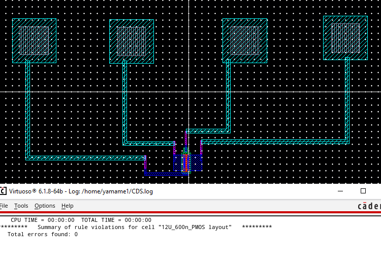
Now we will do the layouts for a 6u/0.6u NMOS and 12u/0.6u PMOS with 4 probe pads connected.
Starting with the NMOS we show the schematic and layout with DRC
Now for the PMOS
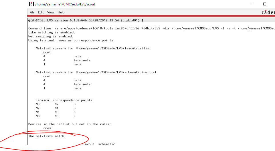
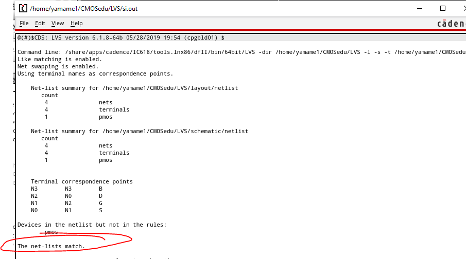
Now we show the LVS for both the NMOS and PMOS
As always I backed up my work
Return to EE 421L Labs