Lab Final Project - EE 421L
Authored
by Cody Woolf
woolfc@unlv.nevada.edu
Today's
date: 21Nov2023
Lab
description:
Project (NOT a group effort) – design a non-inverting buffer circuit that presents less than 100 fF input capacitance to
on-chip logic and that can drive up to a 1 pF load with output voltages greater than 7V (an output logic 0 is near ground
and an output logic 1 is greater than 7V). Assume VDD is between 4.5V and 5.5V, a valid input logic 0 is 1V or less, a valid
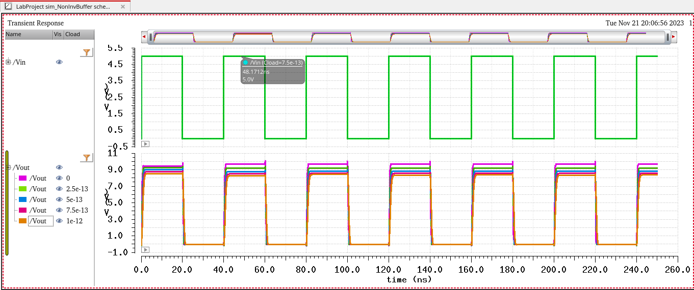
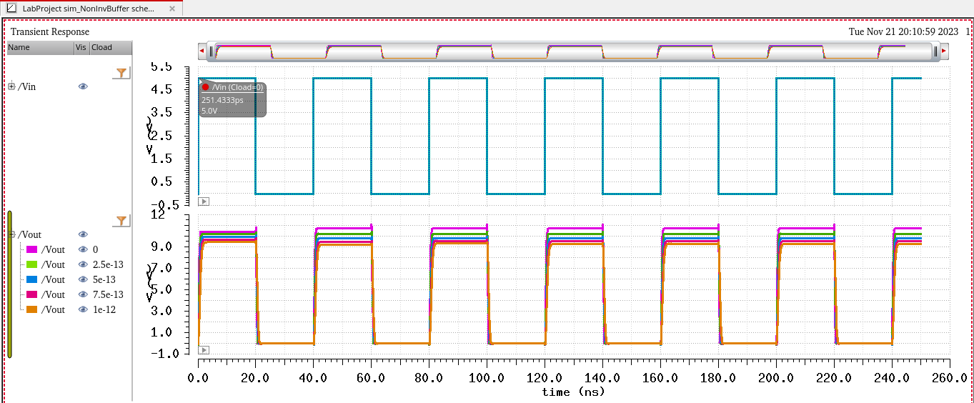
input logic 1 is 3V or more. Show that your design works with varying load capacitance from 0 to 1 pF. Assume the slowest
transition time allowed is 4 ns.
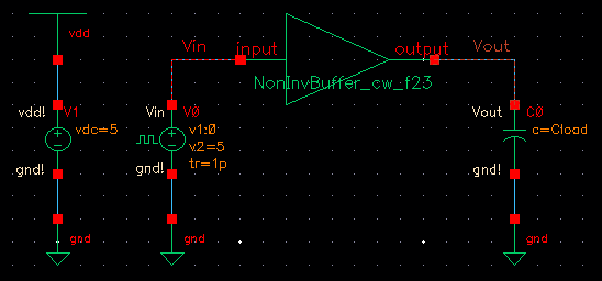
I
will provide the schematic of the designed buffer and go through the
design process; afterwards I will provide the simulations and results
that demonstrate the design criteria are met. While designing the
circuit, simulations were run on this schematic to verify proper
operation. Since a layout is required, once proper operation was
verified, I removed the load, the pulse, and Vdd. A symbol was then
created for use in the simulations after the design discussion.
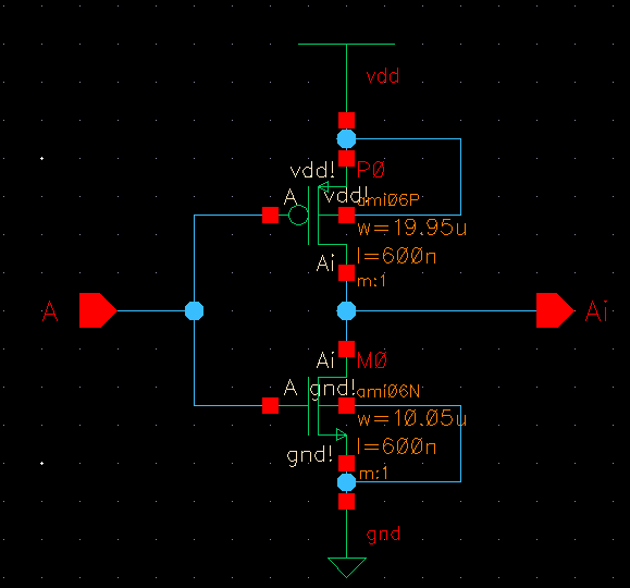
I
began the design process by calculating the size of the first
inverter. I did this by calculating the size of an inverter based of an
assumed resistance value for the PMOS and NMOS. The resistance value I
assumed met the requirements for transistion time.
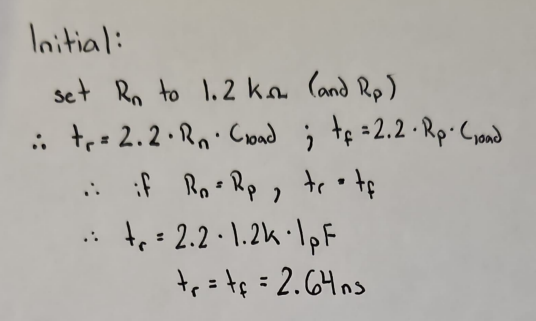
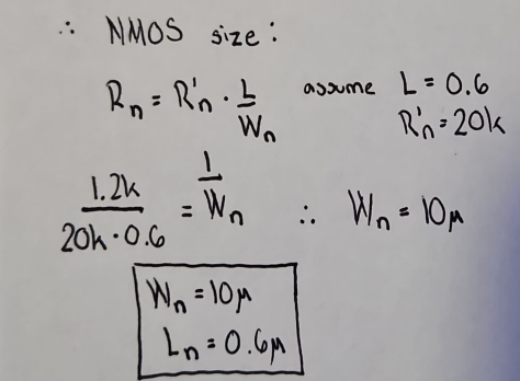
Using
this resistance, I calculated the width of the NMOS assuming a length
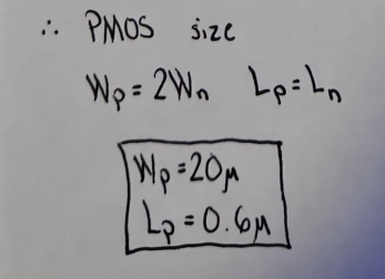
of 0.6um. The width of the PMOS was derived from the width of the NMOS.
Once,
I had the sizes of the MOSFETs in the inverter, I verified that the
input capacitance met the requirements and was less than 100fF.
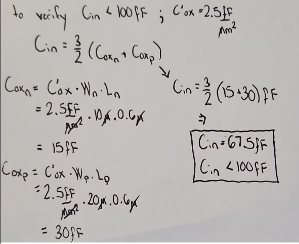
Since
the input capacitance meets the design requirements, I can use the
calculated sizes for my input inverter. The schematic and symbol are
provided below.
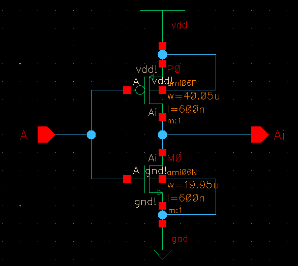
To
ensure I had the proper response, I doubled the size of the input
inverter for the inverter in the circuit that is positioned prior to
the capacitor. The schematic and symbol are provided below.
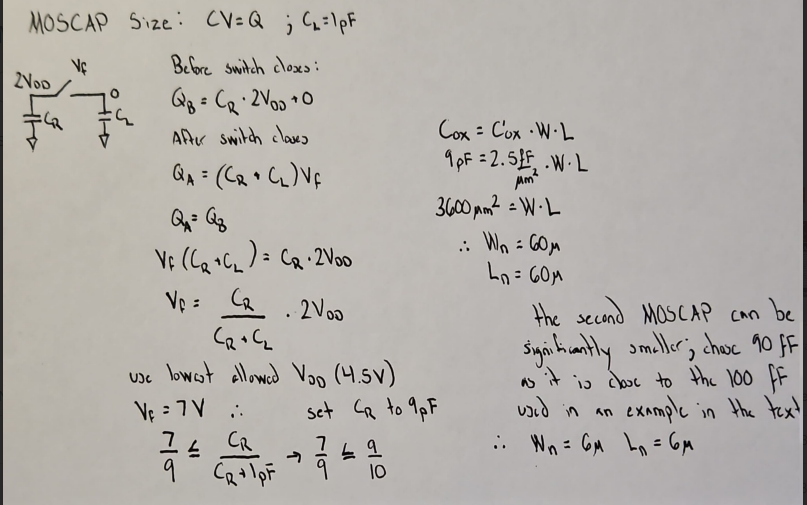
The
capacitor after the above inverter needs to be a certain capacitance so
that the appropriate voltage is driven to the output. The following
calculations give the size of the MOSFET capacitor used. The capacitor
to the left in the circuit can be smaller so a value of 90fF was chosen.
The
two NMOS at the top were arbitrarily chosen; the only requirement was
that the right NMOS be larger than the NMOS on the left. For this I
chose a ratio of 1:5. For the inverter at the output, I redid my
calcuations to ensure a faster response time. The calculations are provided
below.
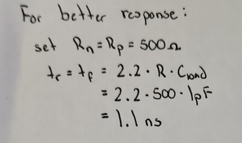
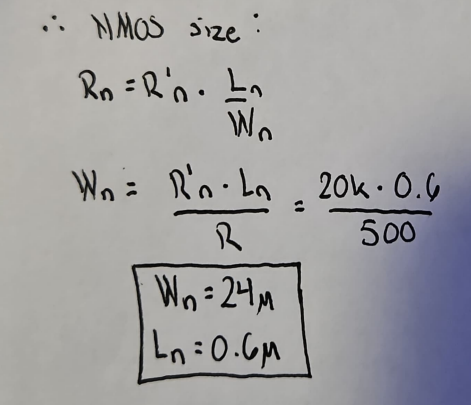
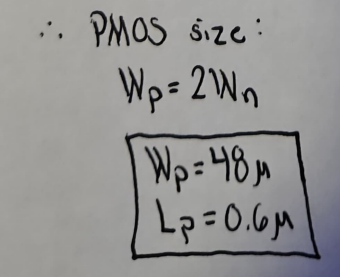
With these values, I sized the inverter at the output.
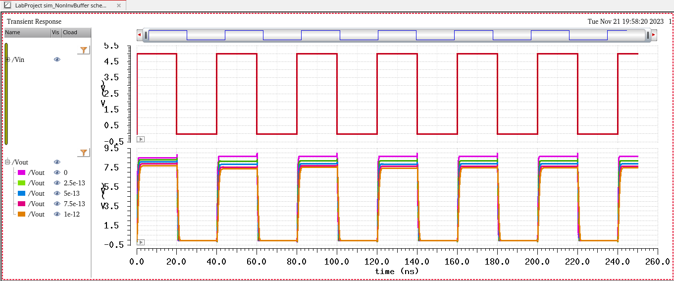
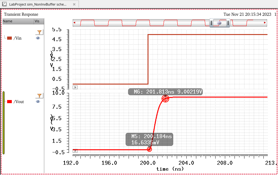
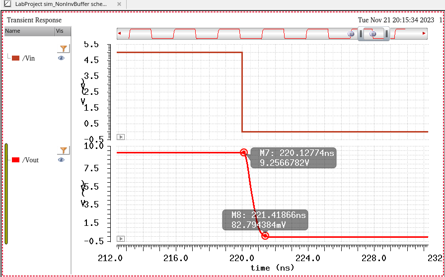
I
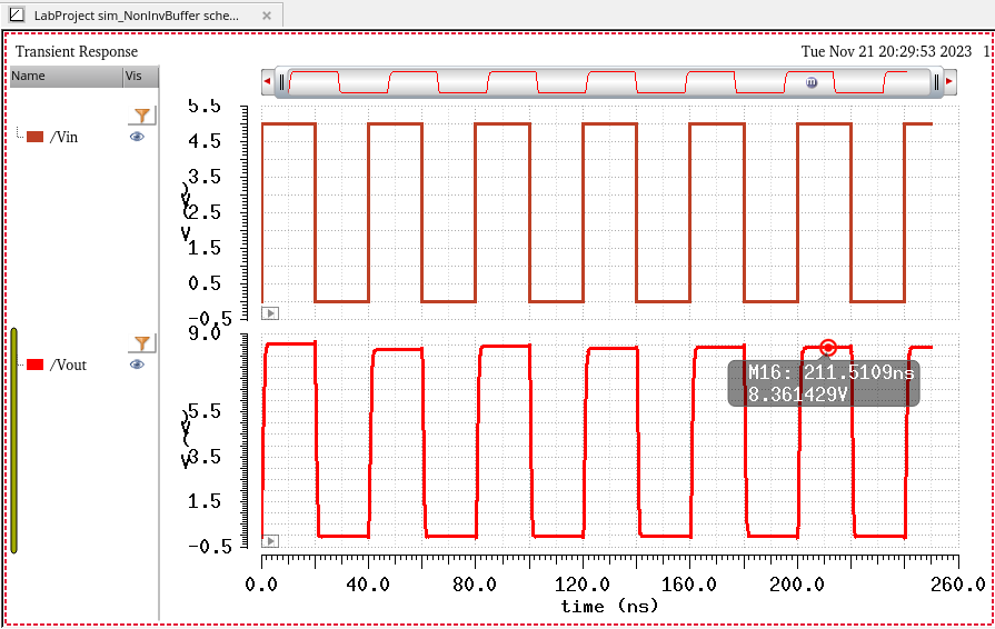
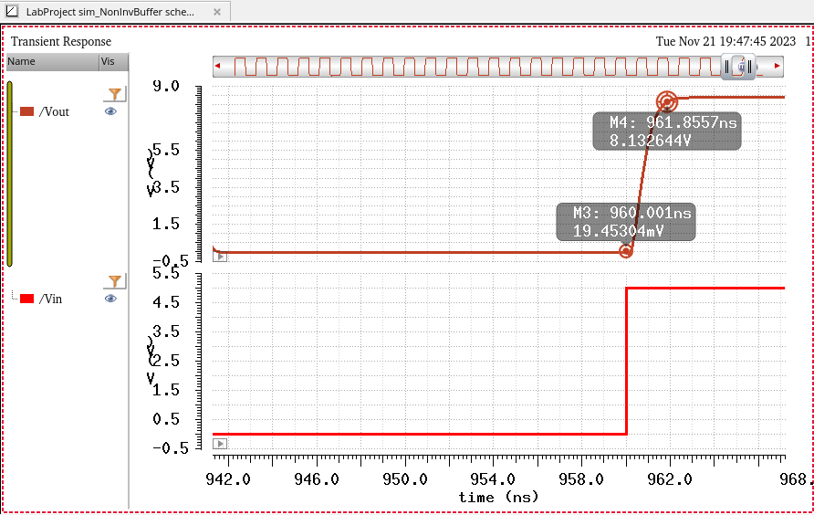
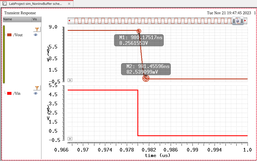
ran simulations at Vdd = 4.5V/5V/5.5V using a parametric analysis. In
the results, I verified the rise and fall time were less than 4ns and
that the output voltage was 7V. As can be seen in the results, the
worst case scenario was at Vdd = 4.5V and a load capacitance of 1pF.
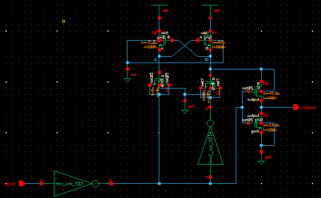
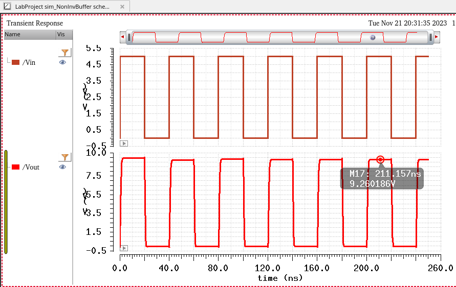
Simulation Schematic:
Simulation results at 4.5V Vdd:
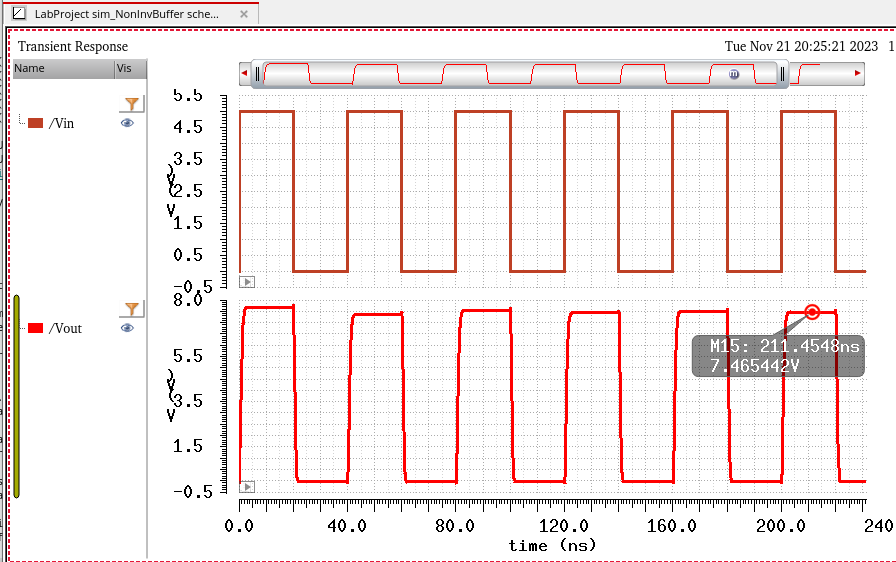
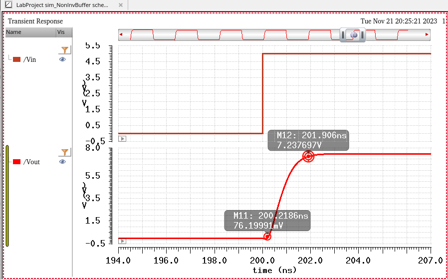
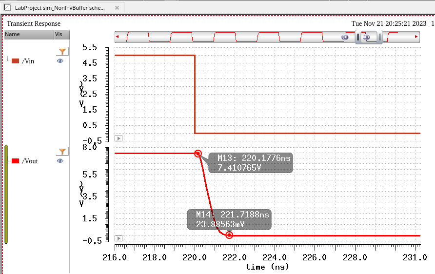
Simulation results at 5V Vdd:
Simulation results at 5.5V Vdd:
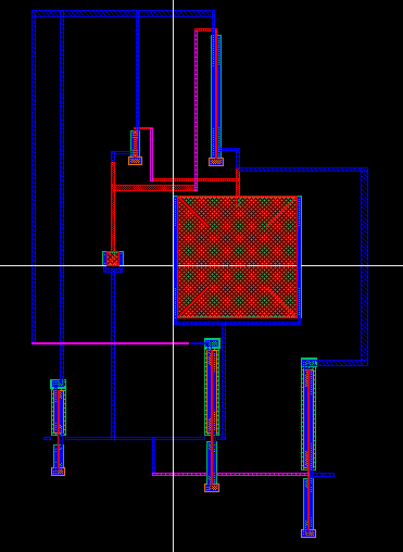
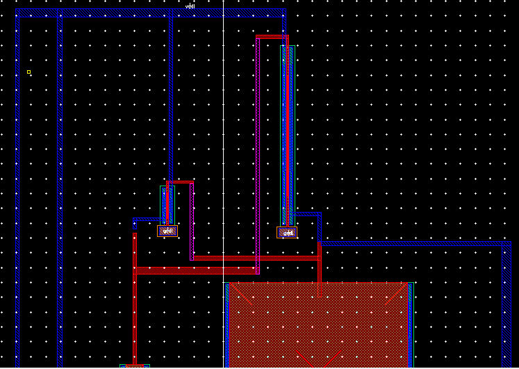
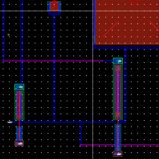
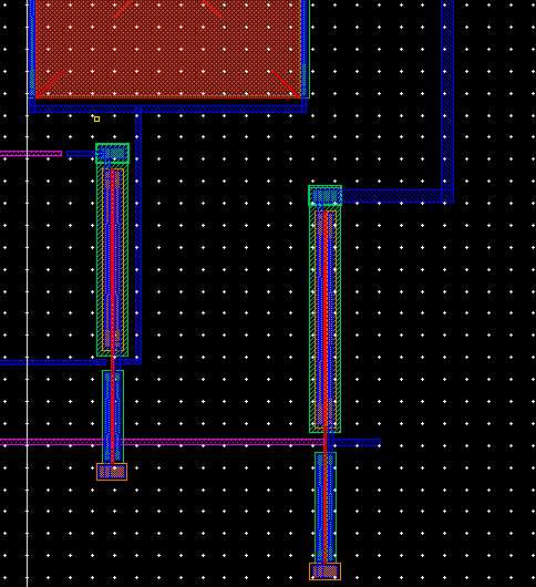
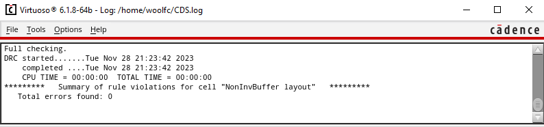
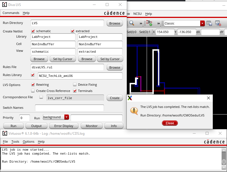
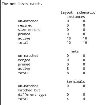
Layout with verified DRC and LVS:
Click to access the files used in this project.
Return to Index