Lab 7 - EE 421L
Authored
by Cody Woolf
woolfc@unlv.nevada.edu
Today's
date: 8Nov2023
Pre-Lab:
Work
remains backed-up from Lab 6; will update with work from this lab.
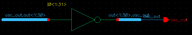
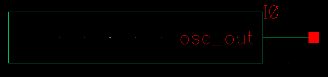
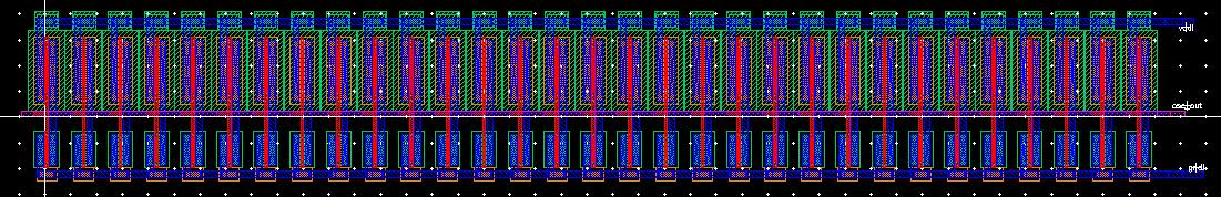
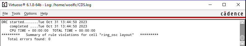
Additionally, we were directed to perform Tutorial 5; this deals with
the construction of a 31 stage ring oscillator.
Schematic:
Symbol:
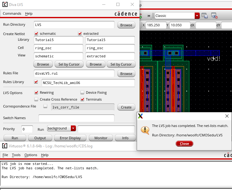
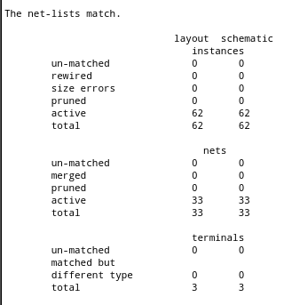
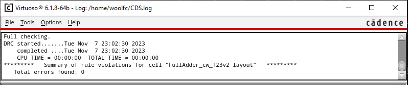
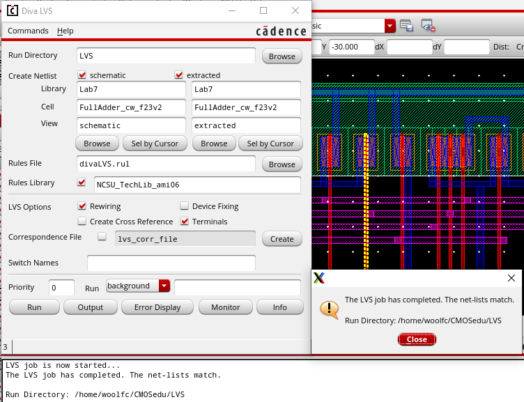
Layout with DRC/LVS:
Lab
description:
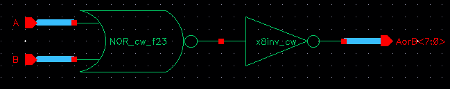
This
lab consists of creating several 8-bit logic gates. Prior to that we
were directed to create a 4-bit inverter and a 2-1 Demux/Mux; we were
directed to provide schematics, symbols, and simulations. The logic
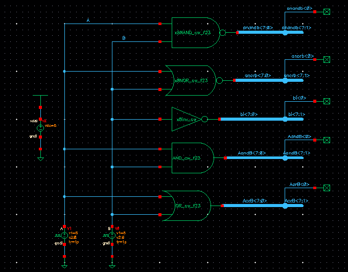
gates in this lab are as follows: inverter, NAND, NOR, AND, OR. A
schematic, symbol, and simulation with results are all required for
each gate; for the simulations I built one schematic and simulated each
gate at once. After the gates, we build an 8-bit 2-1 Demux/Mux with
schematic, symbol, and simulation with results. Last, we created a full
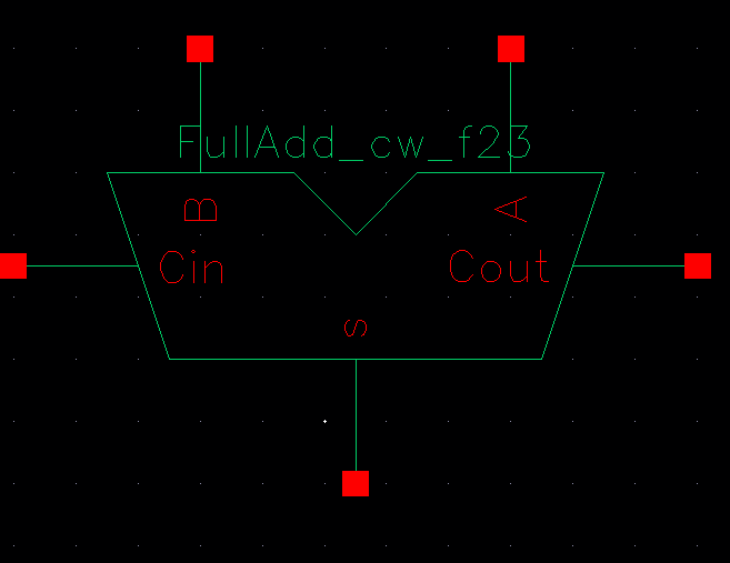
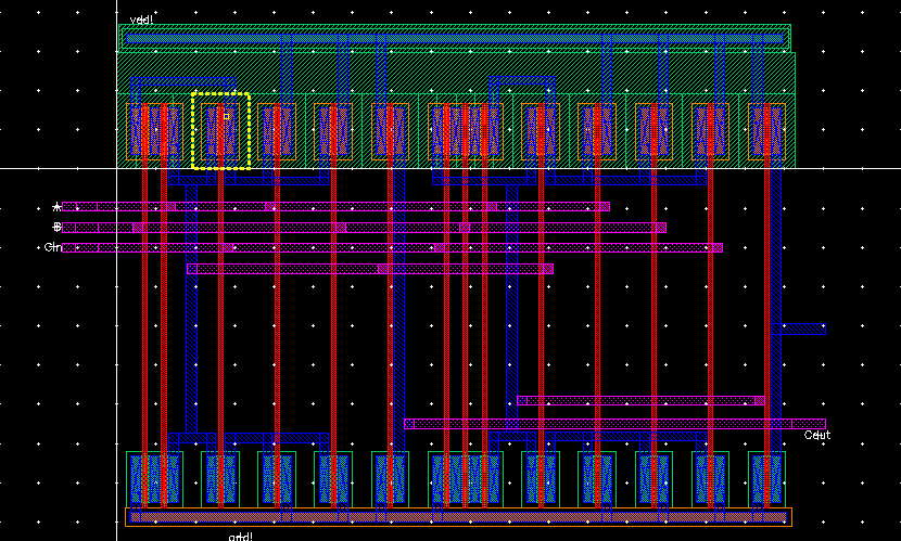
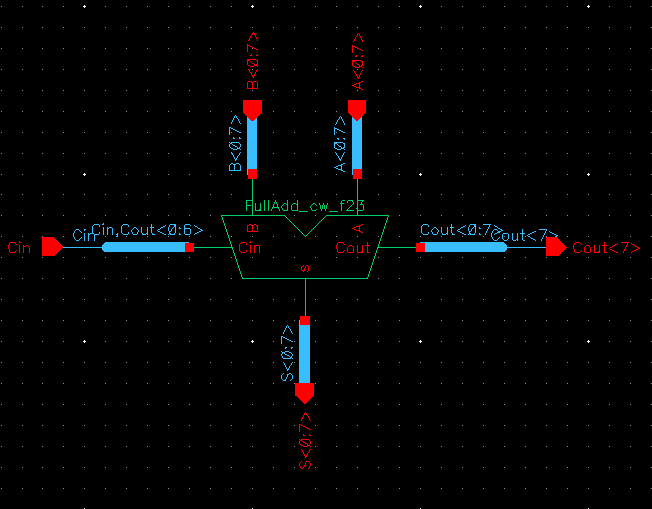
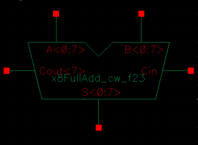
adder schematic, symbol, and layout based off Figure 12.20 from the
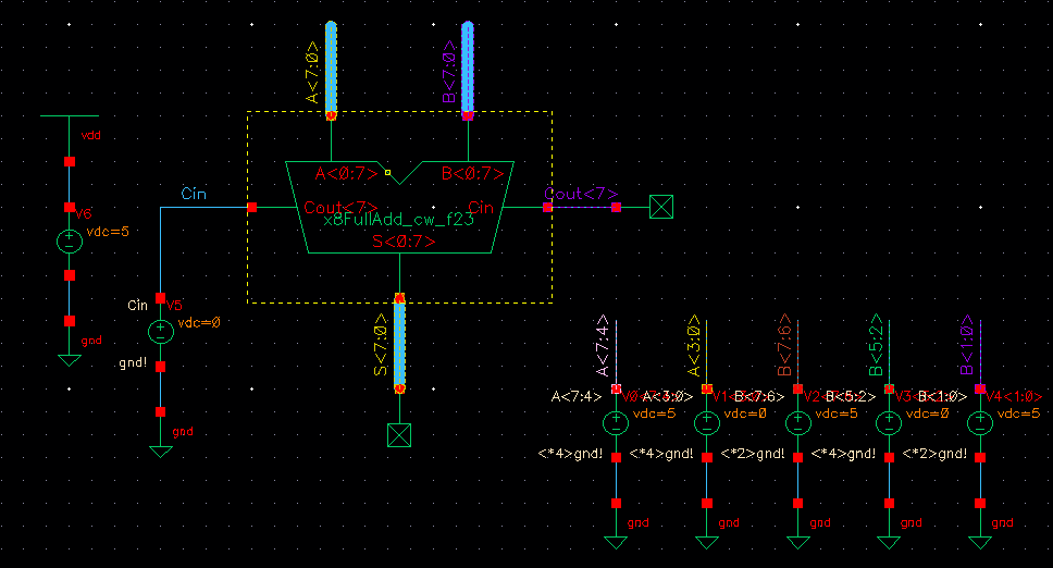
CMOS textbook.Using this, an 8-bit full adder schematic, symbol, layout, and simulation with results was created.
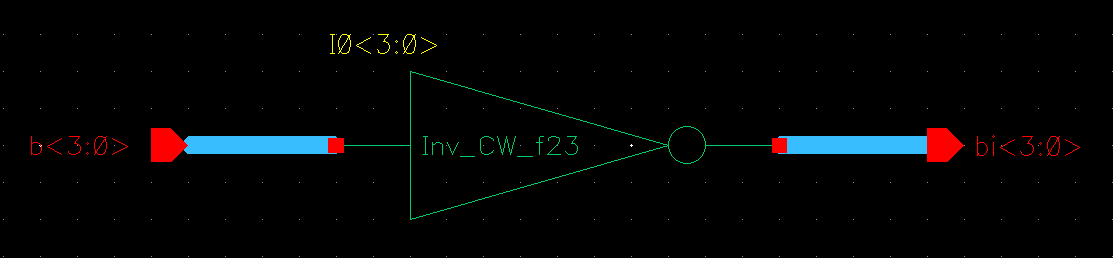
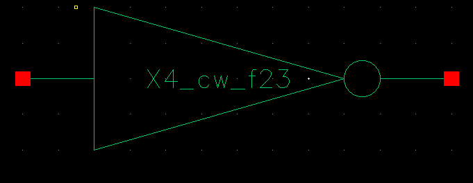
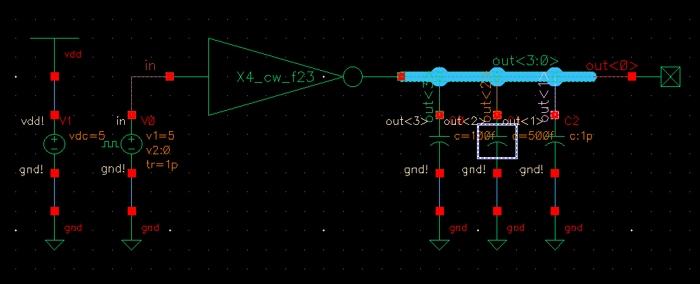
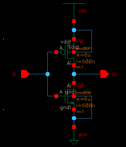
4-bit Inverter:
Schematic:
Symbol:
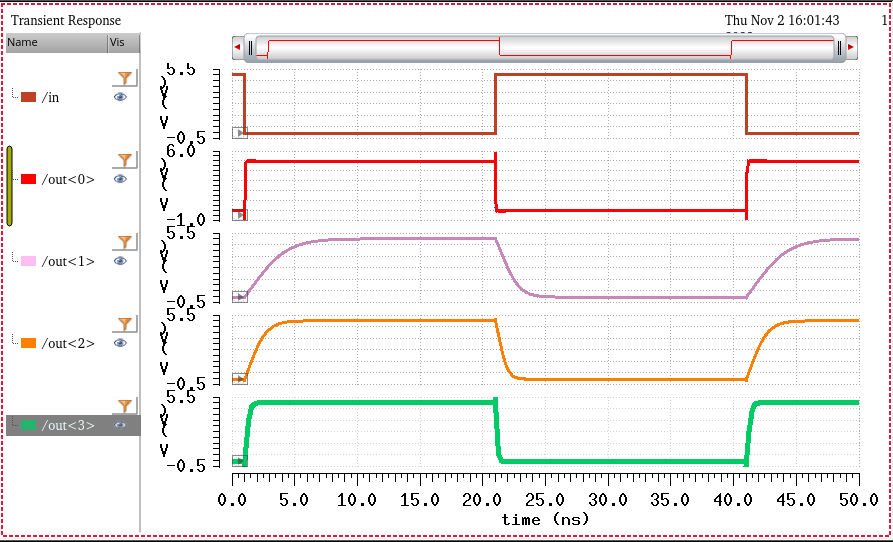
Simulation/Results:
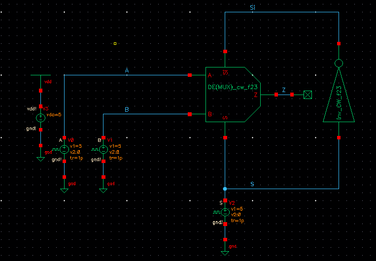
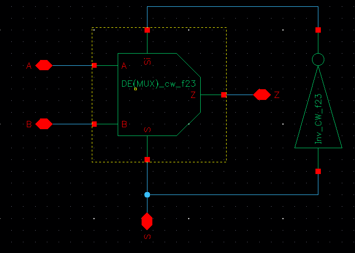
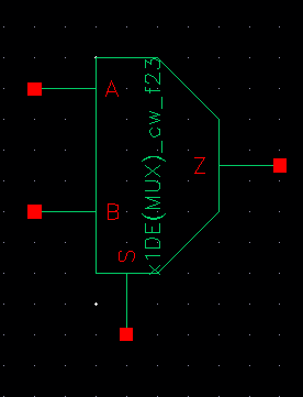
2-1 Demux/Mux:
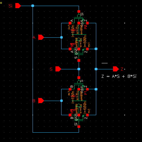
Schematic:
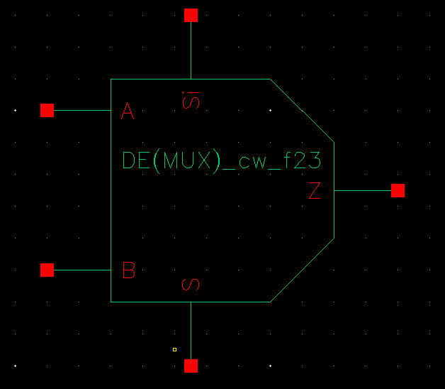
Symbol:
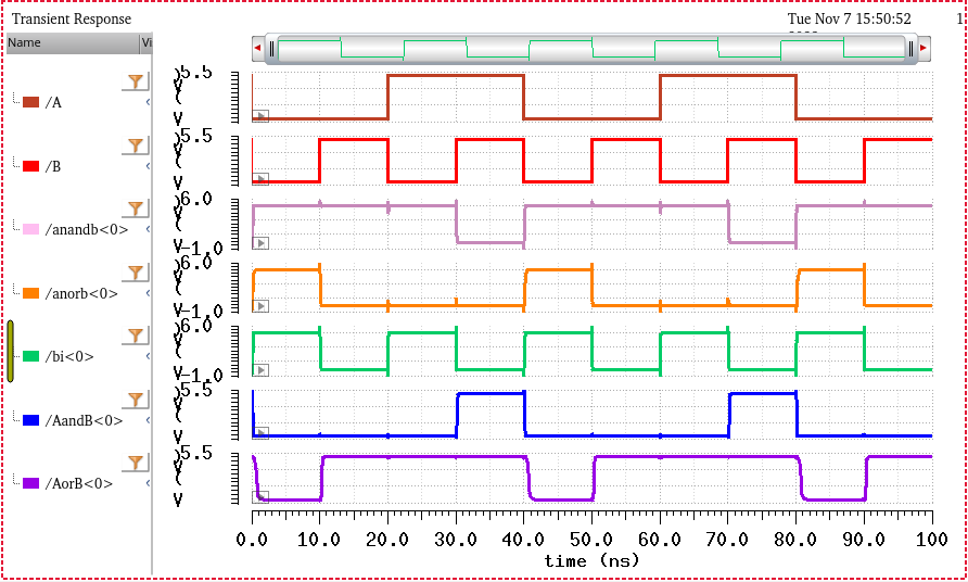
Mux Simulation/Results:
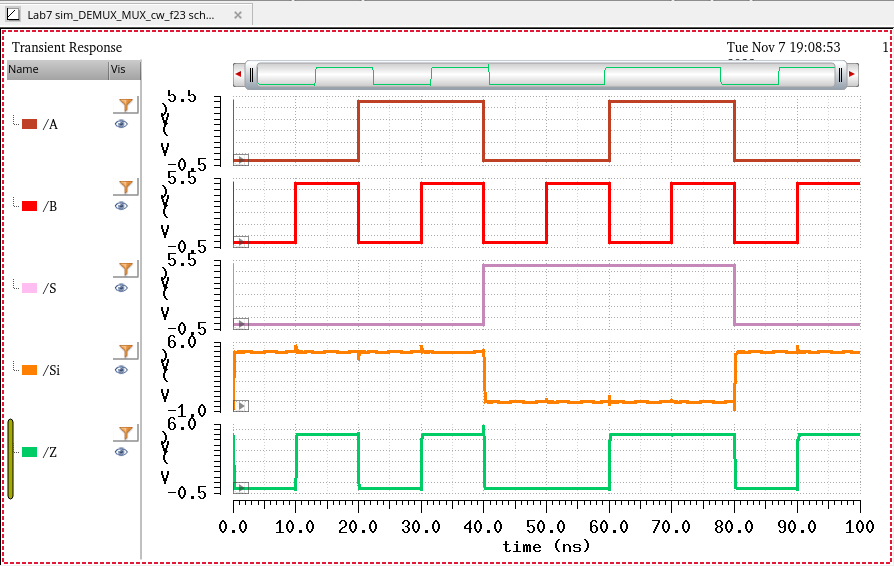
Demux Simulation/Results:
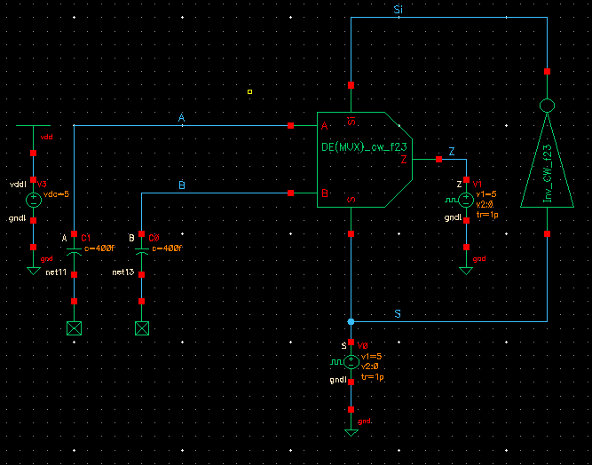
Creation of Symbol for use in 8-bit Demux/Mux:
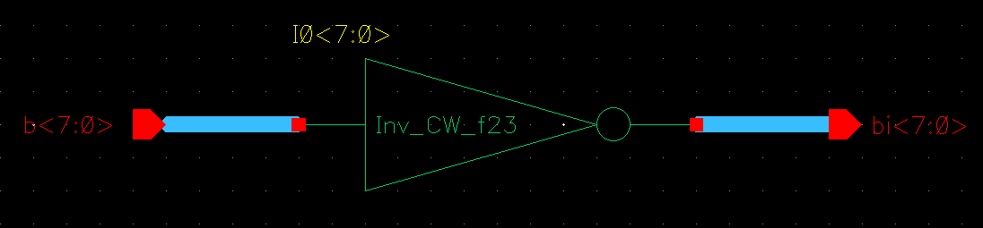
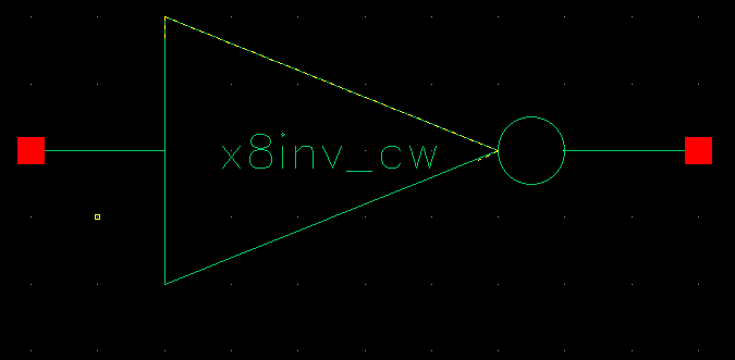
8-bit Inverter:
Schematic:
Symbol:
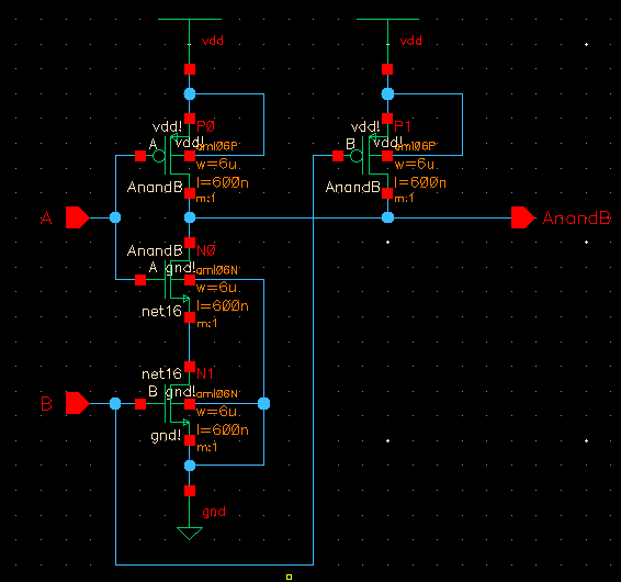
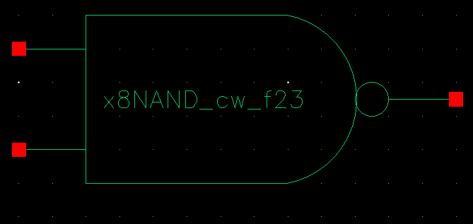
8-bit NAND:
Schematic:
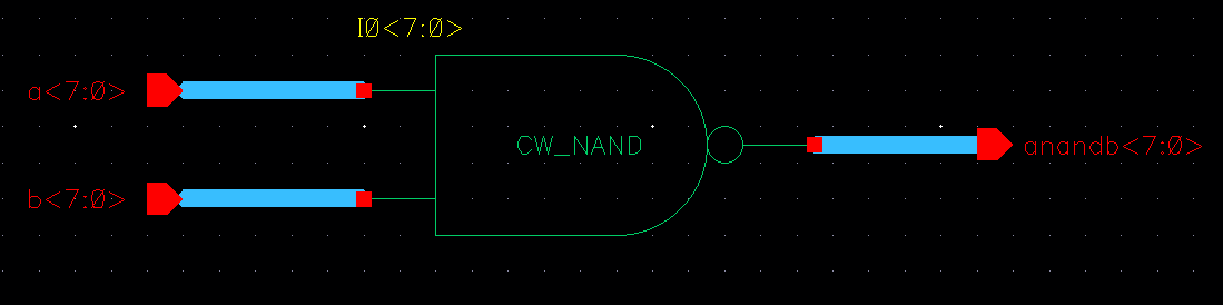
Symbol:
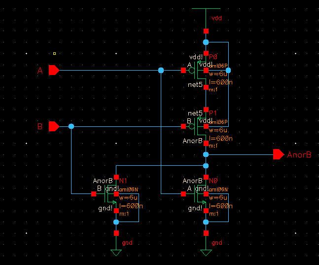
8-bit NOR:
Schematic:
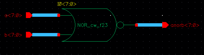
Symbol:
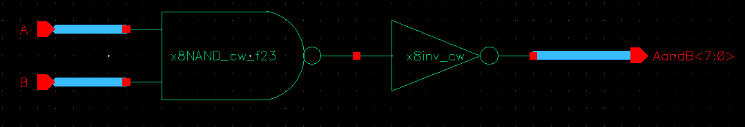
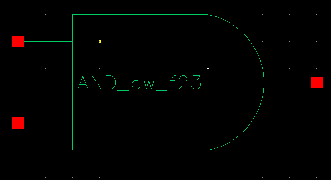
8-bit AND:
Schematic:
Symbol:
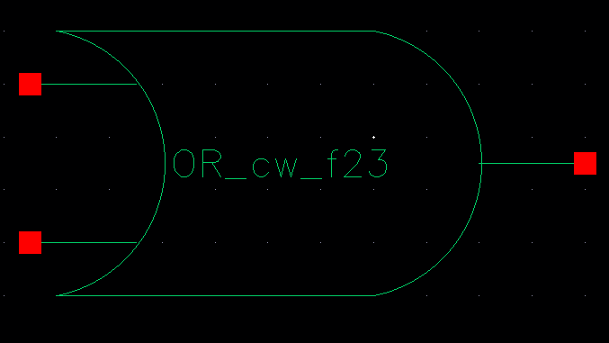
8-bit OR:
Schematic:
Symbol:
Simulation/Results all gates:
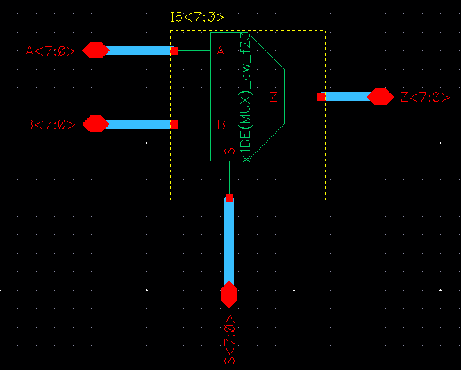
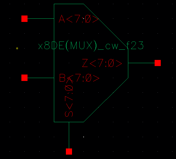
8-bit 2-1 Demux/Mux:
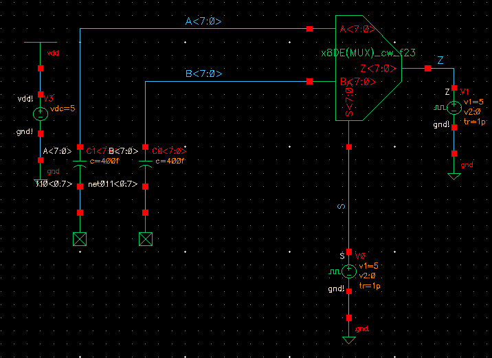
Schematic:
Symbol:
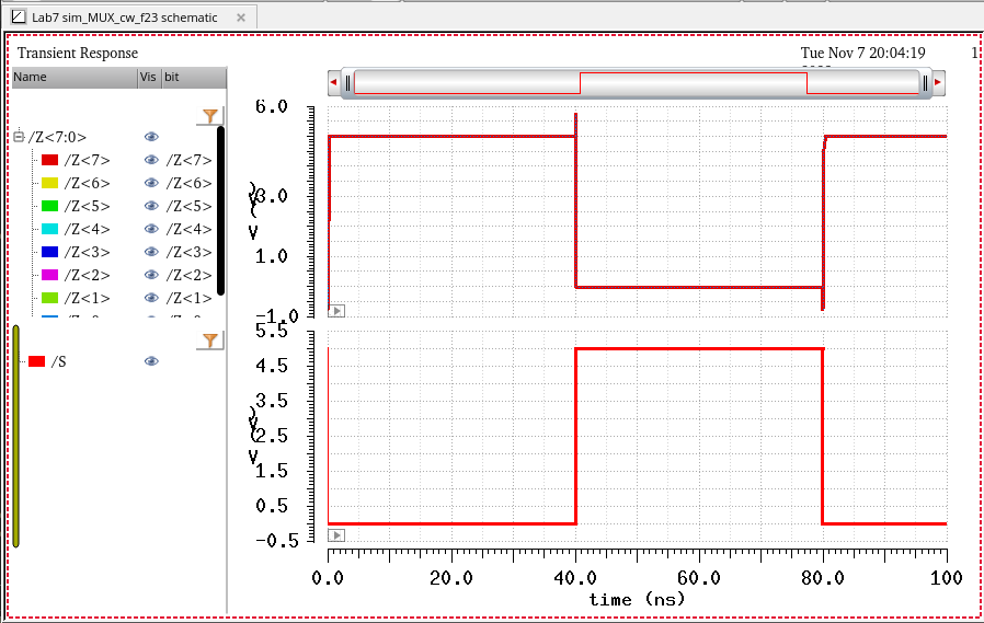
Mux Simulation/Results:
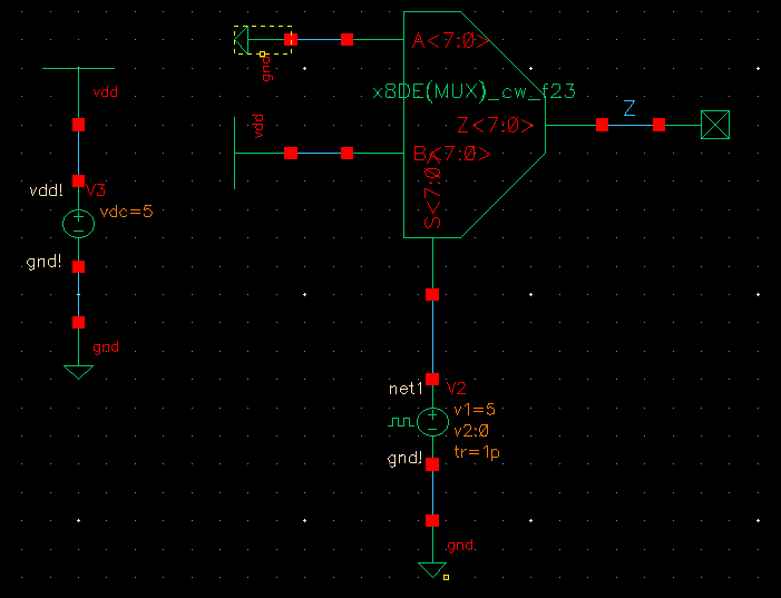
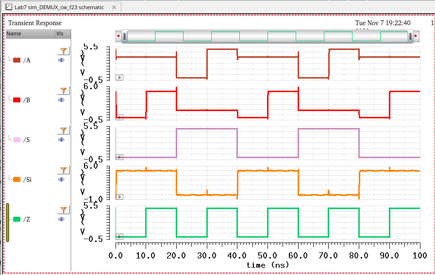
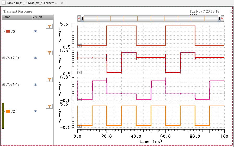
Demux Simulation/Results:
Full Adder:
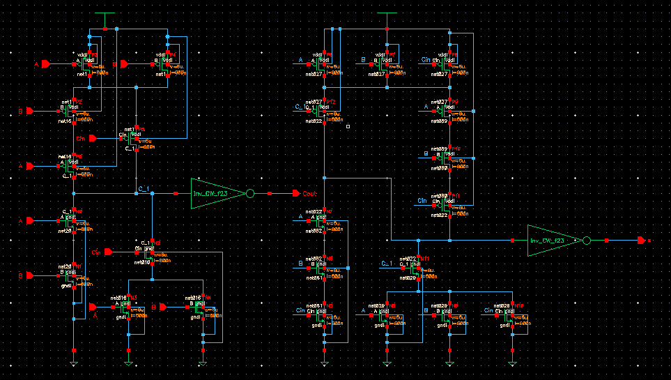
Schematic:
Symbol:
Layout with DRC/LVS:
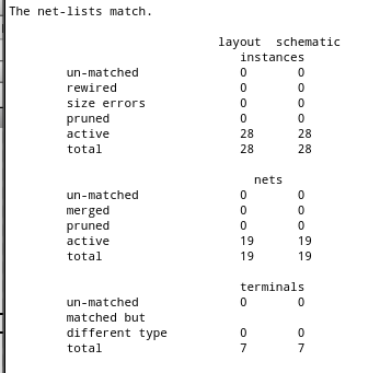
8-bit Full Adder:
Schematic:
Symbol:
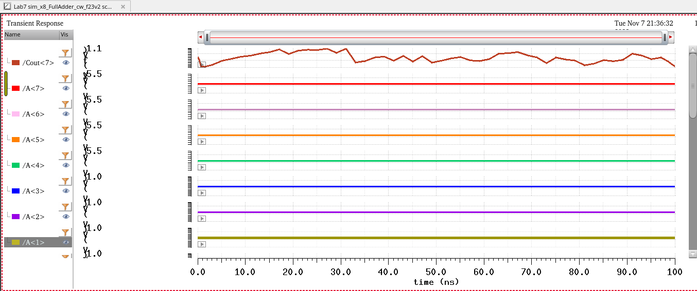
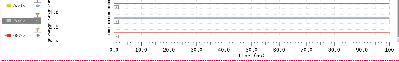
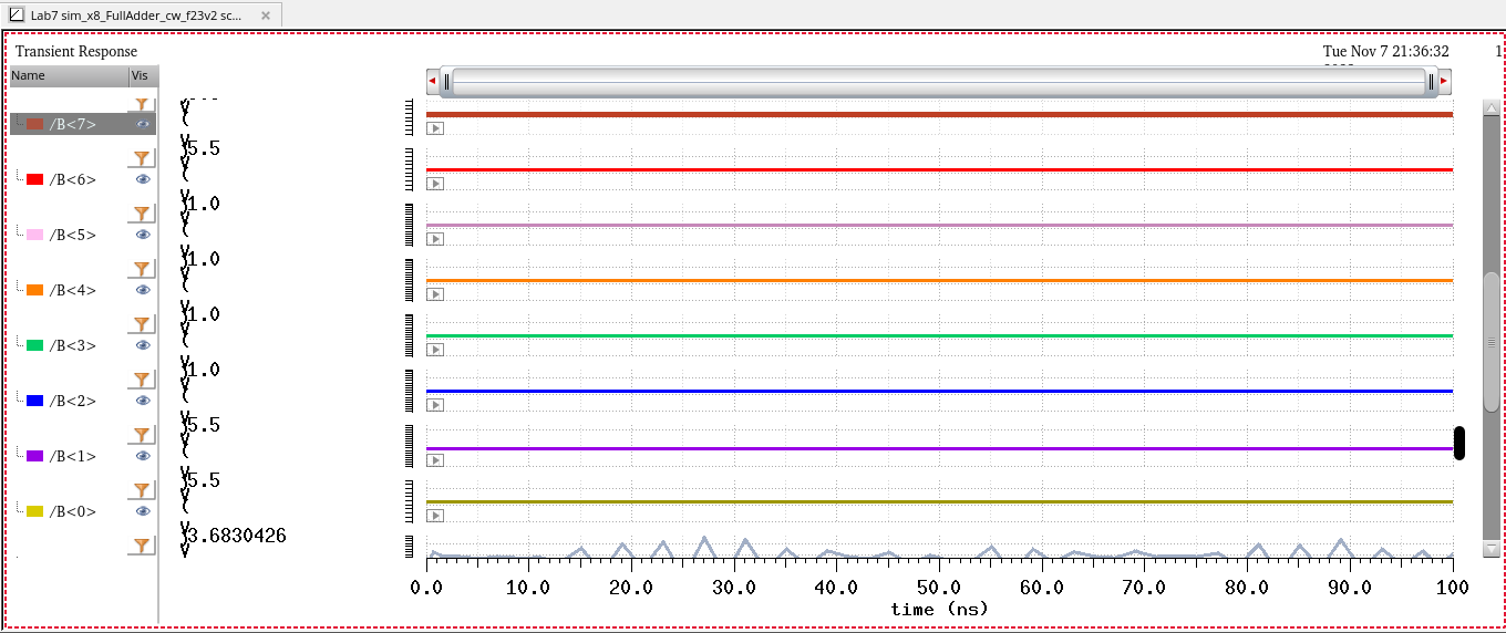
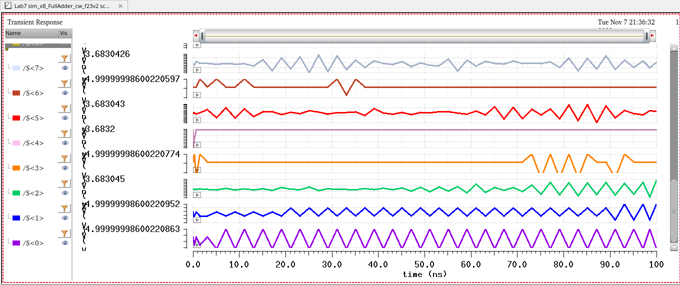
Simulation/Results:
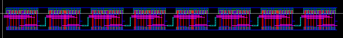
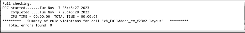
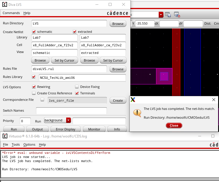
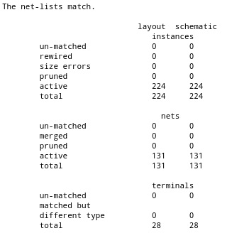
Layout with DRC/LVS:
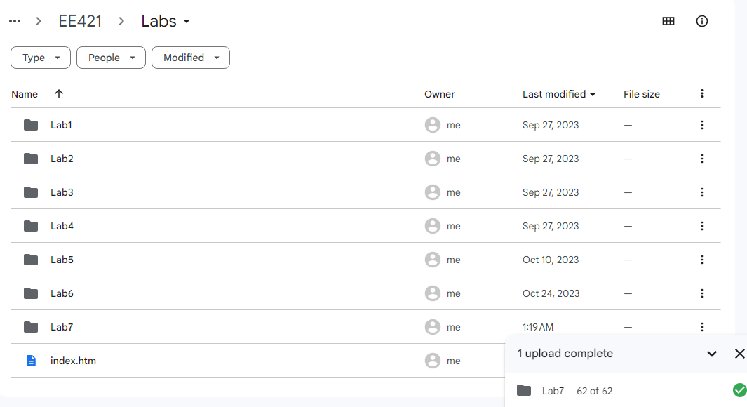
Back-up:
Lab 7 added to Google Drive:
Return to Index