Lab 6 - EE 421L
Authored
by Cody Woolf
woolfc@unlv.nevada.edu
Today's
date: 24Oct2023
Pre-Lab:
Course
and lab work were updated at the end of Lab 5 and no changes occurred
by the pre-lab. At the end of the lab, the new data will be backed-up;
this will be shown at the end of the report.
The
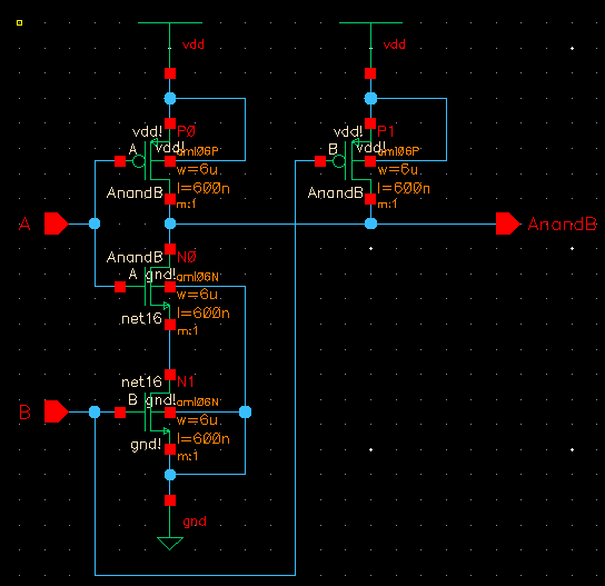
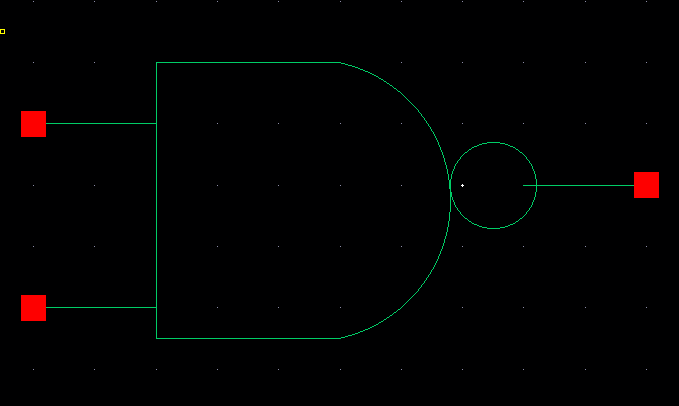
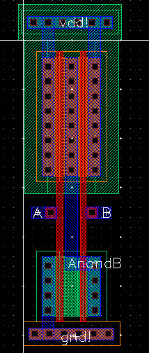
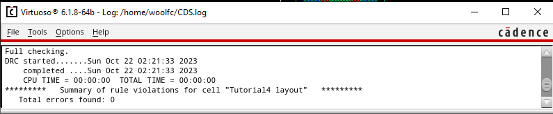
next portion of the pre-lab was to conduct Tutorial 4. In Tutorial 4,
we were directed to create the schematic of a NAND Gate using MOSFETs
then the associated symbol. Afterwards, a layout was generated which
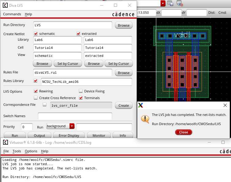
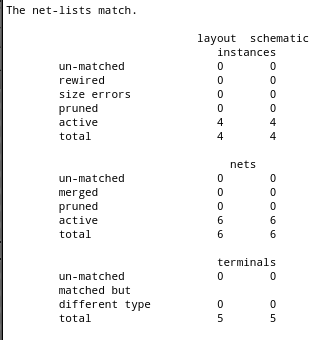
was then verified by DRC and LVS. The tutorial concludes with
simulating the NAND Gate.
NAND Gate Schematic:
NAND Gate Symbol:
NAND Gate Layout:
NAND Gate DRC and LVS:
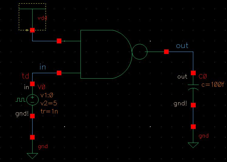
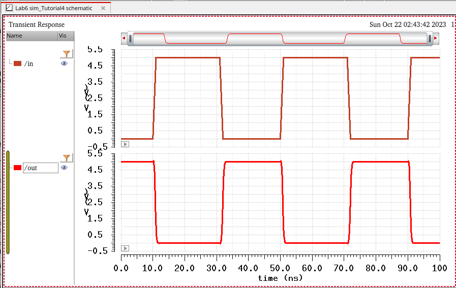
Tutorial 4 Simulation Schematic and Results:
_______________________________________________________________________________________________________________________
Lab Description:
In
this lab, the objective is to build the schematic, symbol, and layout
for each of the following: NAND Gate, XOR Gate, and a Full Adder which
is the combination of NAND and XOR Gates. Each layout will be verified
with a clean DRC and LVS. Simulations will be run for each component
matching the associated truth table.
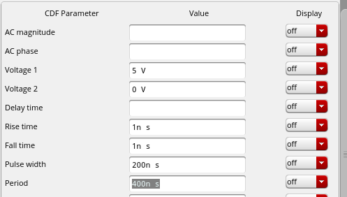
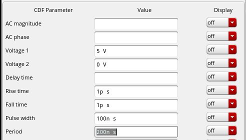
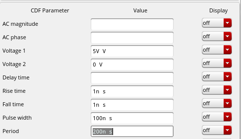
Voltage Pulse Setup:
For NAND and XOR:
A:
B:
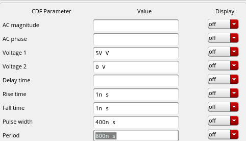
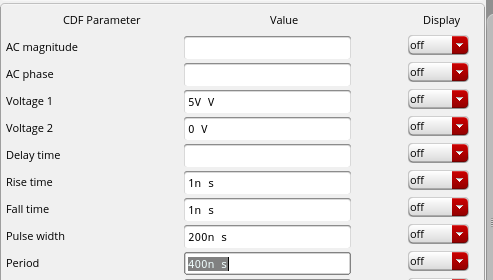
For Full Adder:
A:
B:
C:
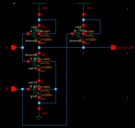
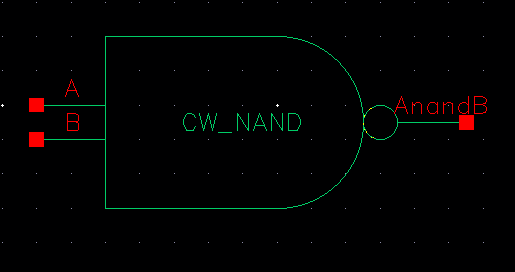
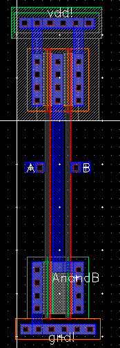
NAND Gate:
Schematic:
Symbol:
Layout:
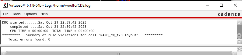
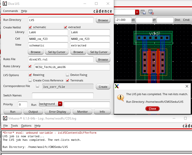
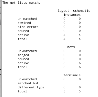
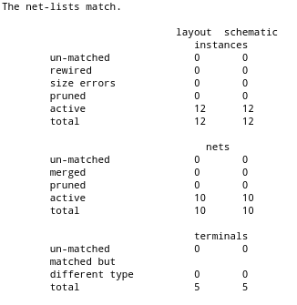
DRC and LVS:
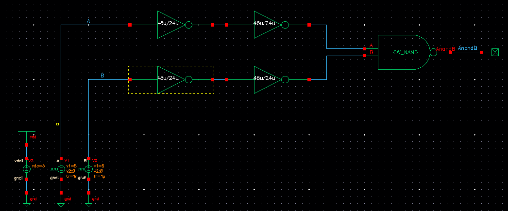
Simulation Schematic and Results:
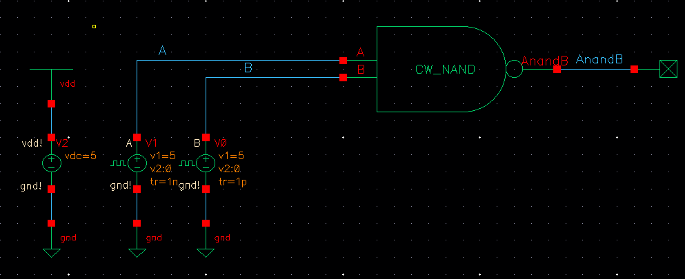
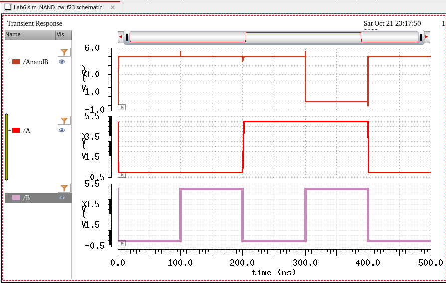
As can be observed in the output,
AnandB, there are spikes in the graph as a result of variations in the
signal. By using inverters, those spikes can be minimized; this will be
applied to all subsequent simulations.
Truth Table(NAND):
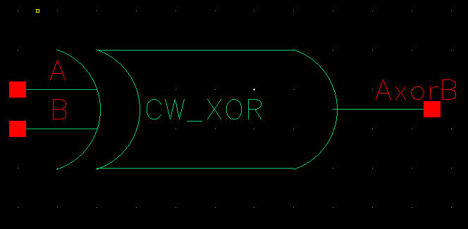
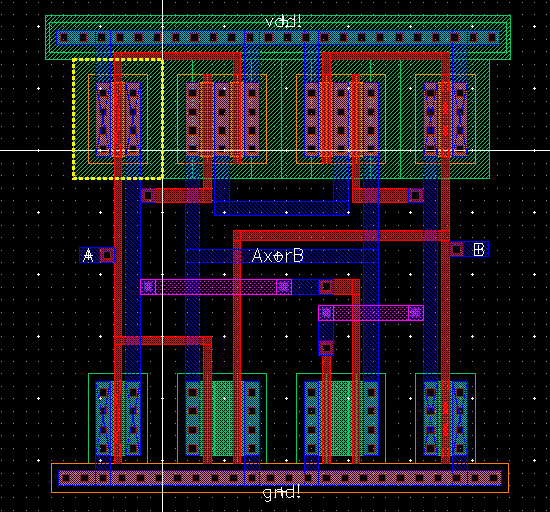
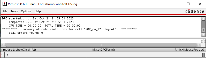
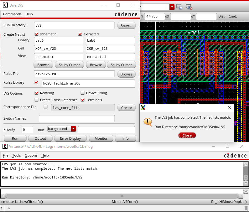
XOR Gate:
Schematic:
Symbol:
Layout:
DRC and LVS:
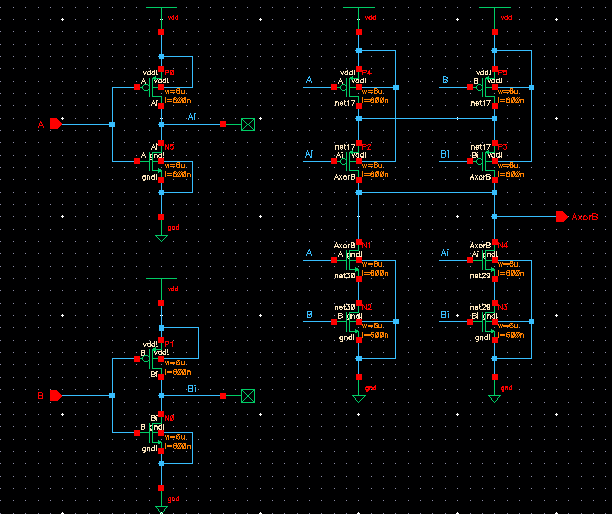
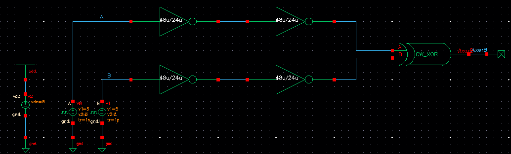
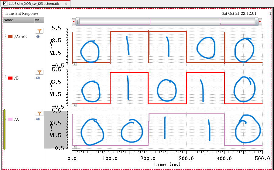
Simulation Schematic and Results:
Truth Table(XOR):
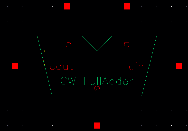
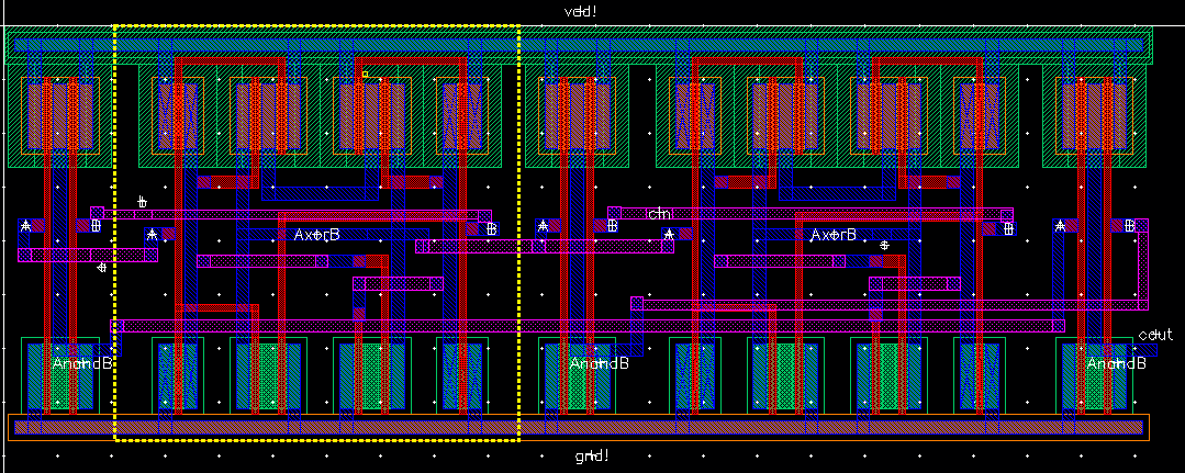
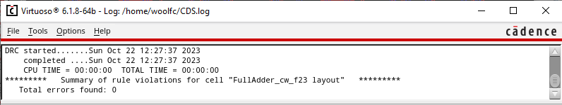
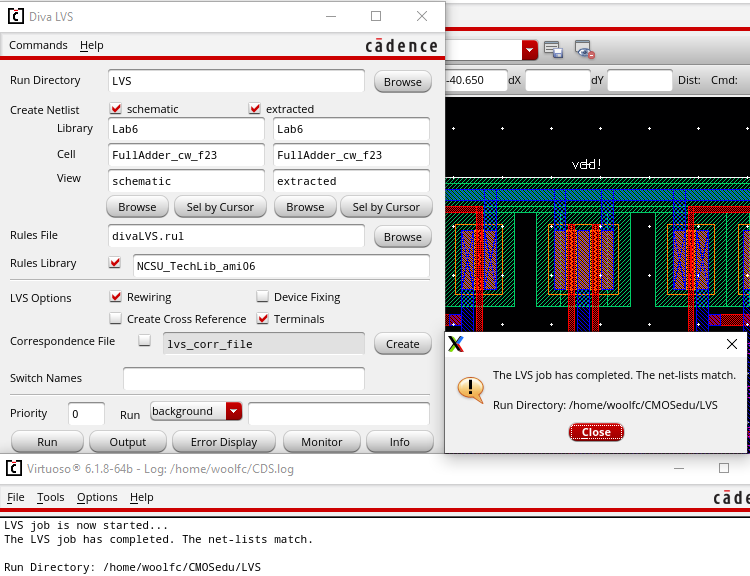
Full Adder:
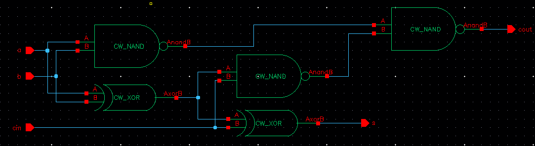
Schematic:
Symbol:
Layout:
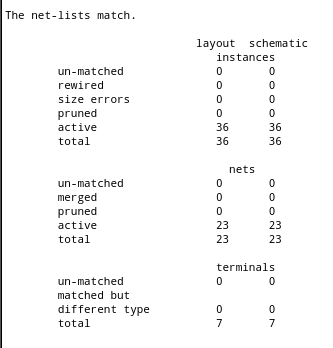
DRC and LVS:
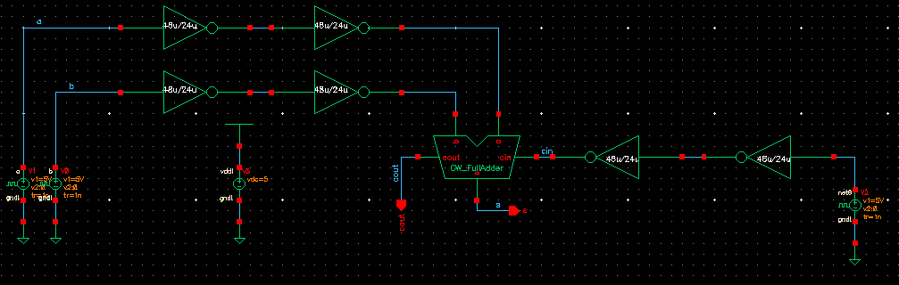
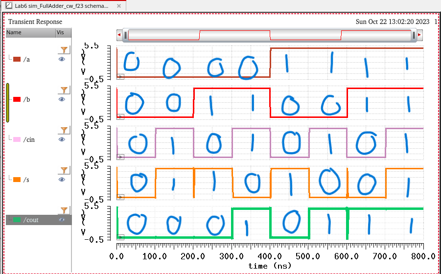
Simulation Schematic and Results:
Truth Table(Full Adder):
| A | B | Cin | s | Cout |
| 0 | 0 | 0 | 0 | 0 |
| 0 | 0 | 1 | 1 | 0 |
| 0 | 1 | 0 | 1 | 0 |
| 0 | 1 | 1 | 0 | 1 |
| 1 | 0 | 0 | 1 | 0 |
| 1 | 0 | 1 | 0 | 1 |
| 1 | 1 | 0 | 0 | 1 |
| 1 | 1 | 1 | 1 | 1 |
Proof of appropriate cell names:
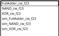
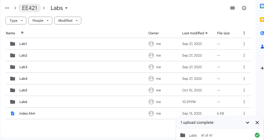
Proof of back-up:
Lab6 file added to Google Drive.
Return to Index