Lab 5 - EE 421L
Authored
by Cody Woolf woolfc@unlv.nevada.edu
Today's
date: 10Oct2023
Pre-Lab:
Back-up:
Questions:
1) What does bindkey q do?
Opens object parameters for editing.
2) What two cell views are used when doing a LVS?
Layout and Schematic.
3) What is the difference between nmos and nmos4 schematic cells?
The nmos4 schematic has the bulk connection whereas nmos does not.
4) How do you select the MOSFET models in the ADE window? What does ADE stand for?
The path for selecting models is as follows:
/$HOME/ncsu-cdk-1.6.0.beta/models/spectre/standalone/ami06N.m (or
ami06P.m).
It stands for Analog Design Environment
5) What is the difference between moving and stretching?woolfc@unlv.nevada.edu
Moving moves the object while stretching changes the physical dimensions of the object.
6) How do you layout a rectangle on the metal1 layer?
Select metal1 in the layer window, press R, then use the mouse to draw the rectangle.
7) What does the ! indicate at the end of gnd! and vdd!?
It indicates a global variable/net.
8) What do the acronyms LSW and CIW stand for?
LSW is Layer Selection Window and CIW is Command Interpreter Window.
9) How is the ruler used? Cleared?
To use the rule press K and to clear press shift+K.
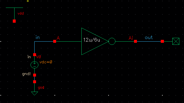
Tutorial 3 guided us in building an inverted and running simulations with it.
It starts with the inverter shcematic.
Next was creating the symbol.
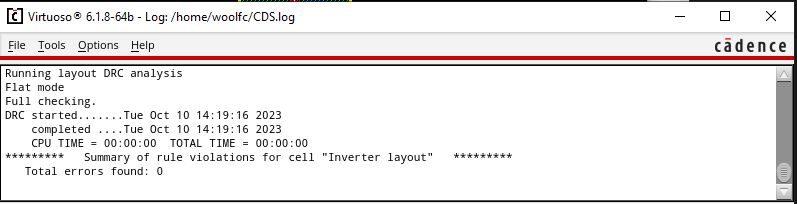
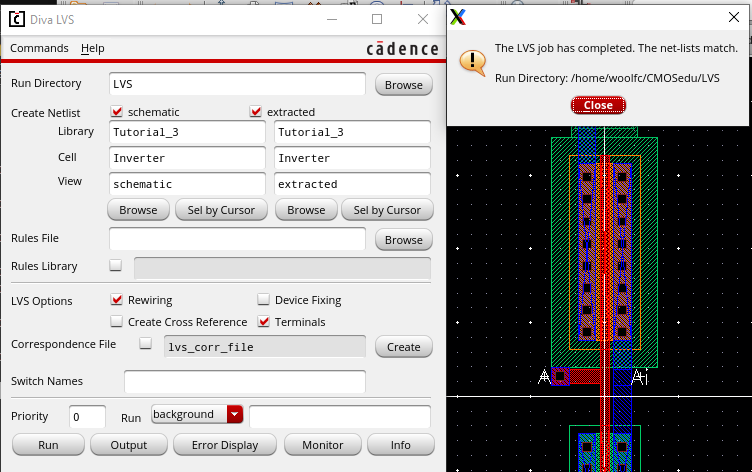
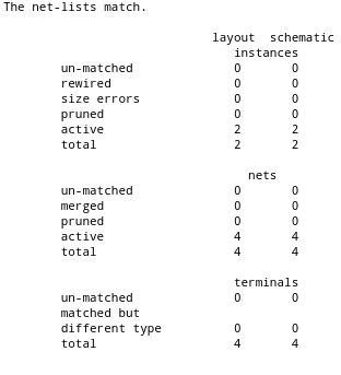
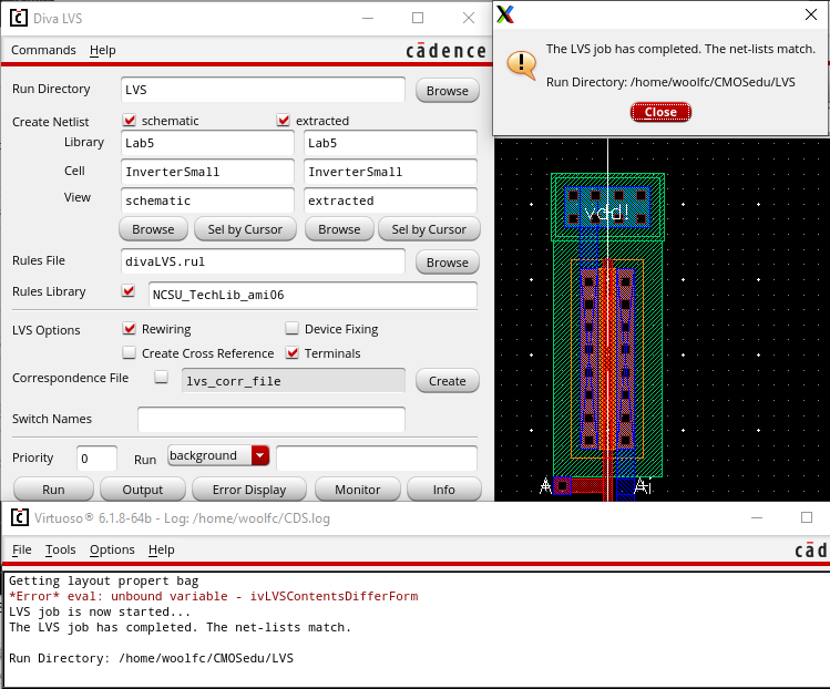
Then the layout was created, verified with DRC, extracted, and a LVS was run.
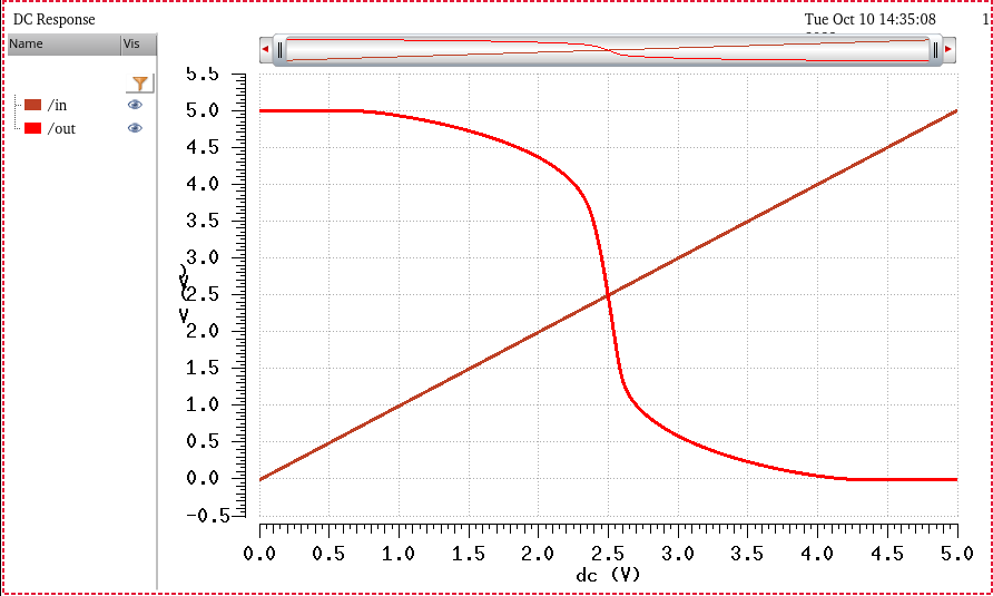
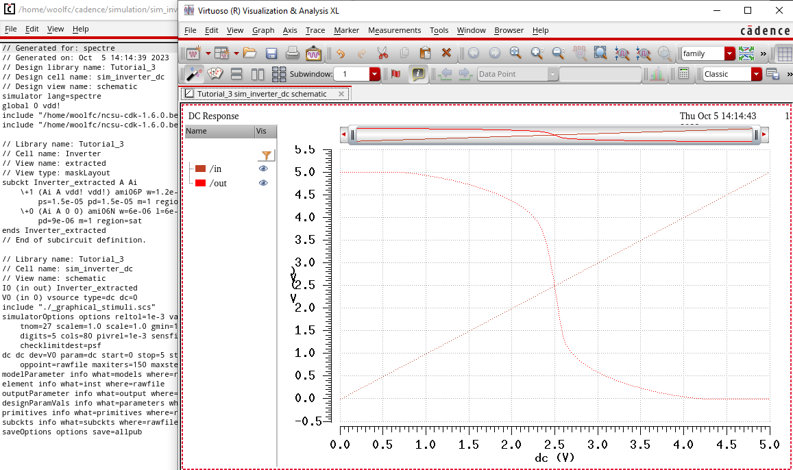
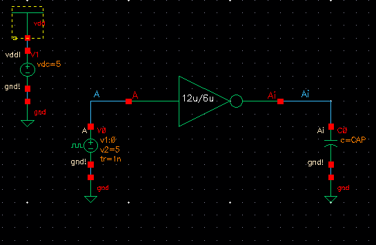
A
circuit using the above inverter was then created and a dc analysis was
run twice. The first was on the schematic and the second was on the
extracted.
______________________________________________________________________________________________________________________________________________________
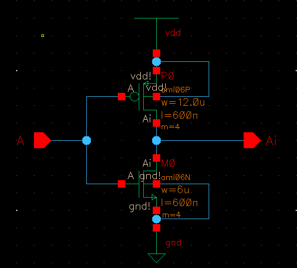
Lab Description:
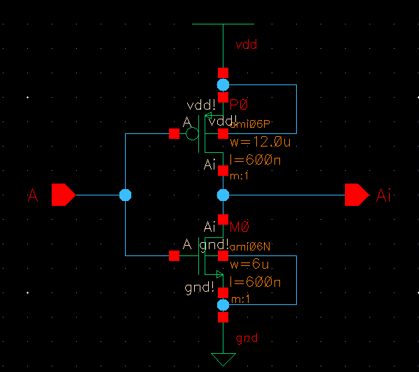
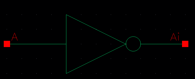
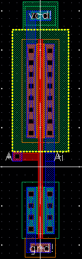
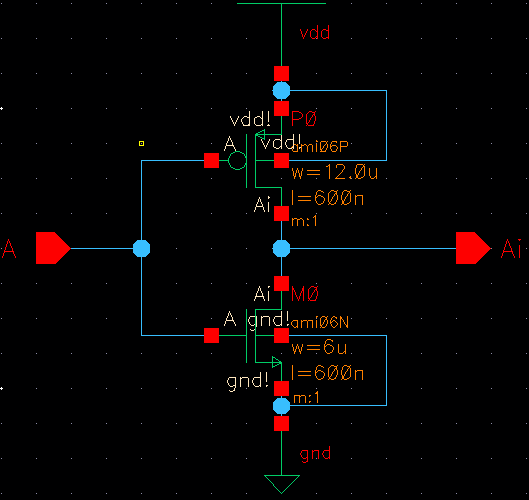
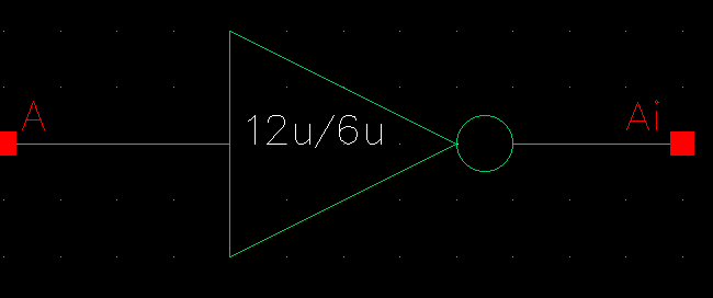
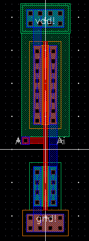
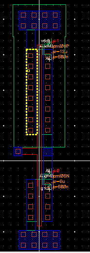
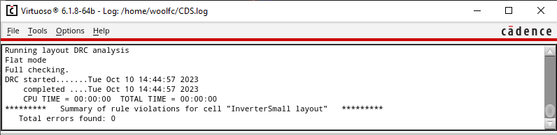
We
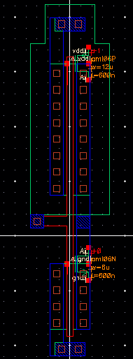
created a 12u/6u inverter schematic, symbol, and layout. The layout was
extracted so we could perform a LVS; the layout was verified with a
DRC.
Schematic:
Symbol:
Layout and Extracted:
DRC:
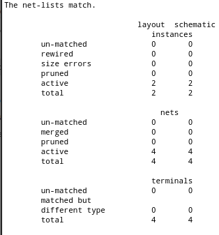
LVS:
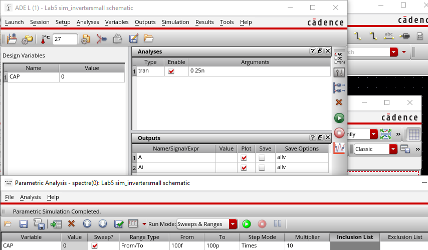
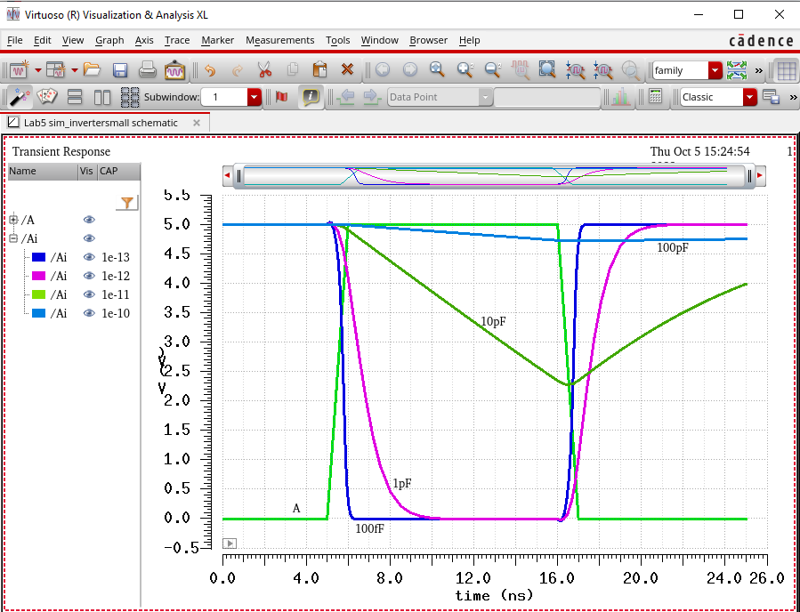
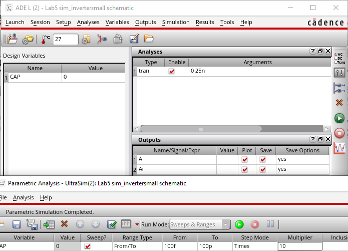
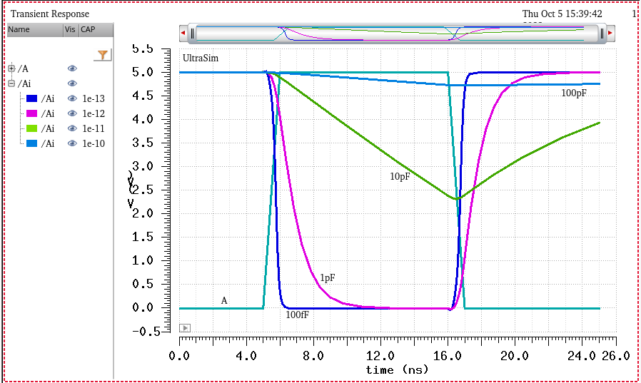
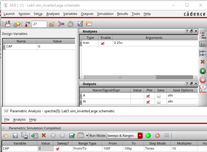
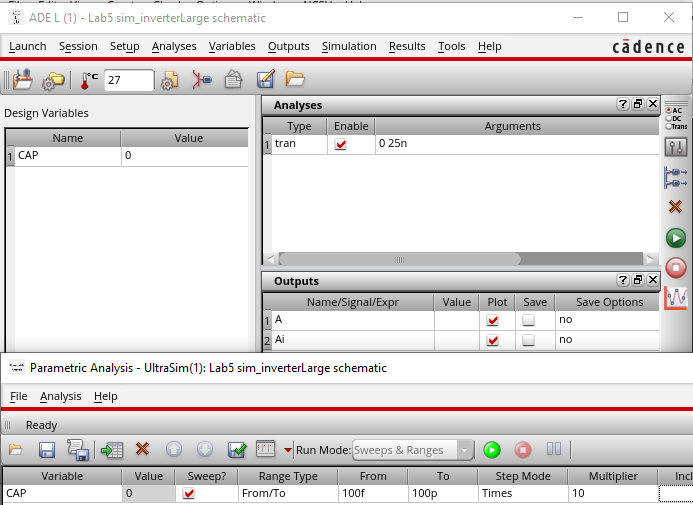
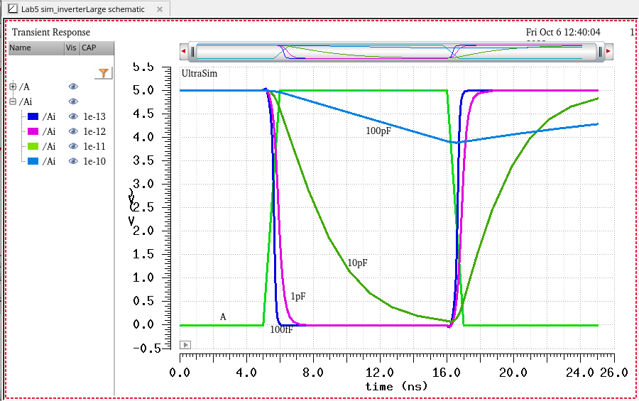
Using
this inverter, two simulations were run using parametric analysis to
sweep the capacitor from 100fF-1pF-10pF-100pF. The first simulation was
a standard .tran analysis using spectre and the second was a transient
analysis using UltraSim from the ADE window.
Schematic:
Results:
Spectre:
UltraSim:
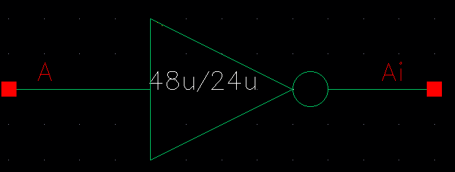
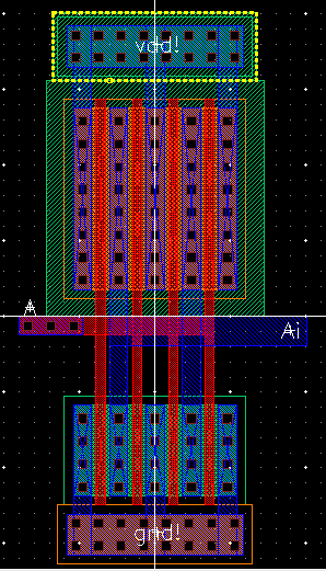
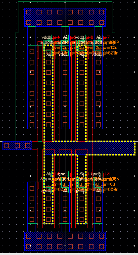
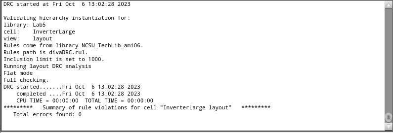
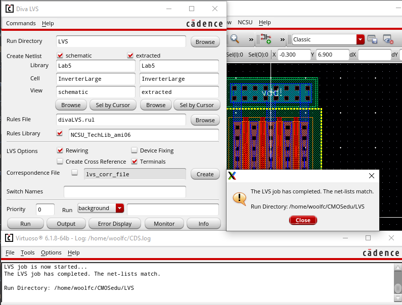
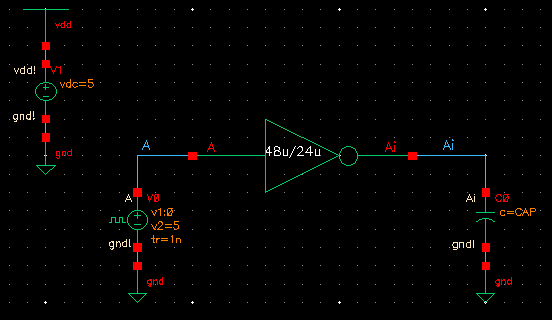
We
created a 48u/12u inverter schematic, symbol, and layout. The layout was
extracted so we could perform a LVS; the layout was verified with a
DRC.
Schematic:
Symbol:
Layout and Extracted:
DRC:
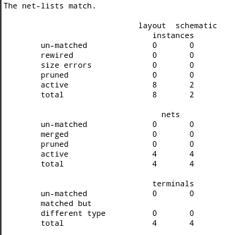
LVS:
Using
this inverter, two simulations were run using parametric analysis to
sweep the capacitor from 100fF-1pF-10pF-100pF. The first simulation was
a standard .tran analysis using spectre and the second was a transient
analysis using UltraSim from the ADE window.
Schematic:
Results:
Spectre:
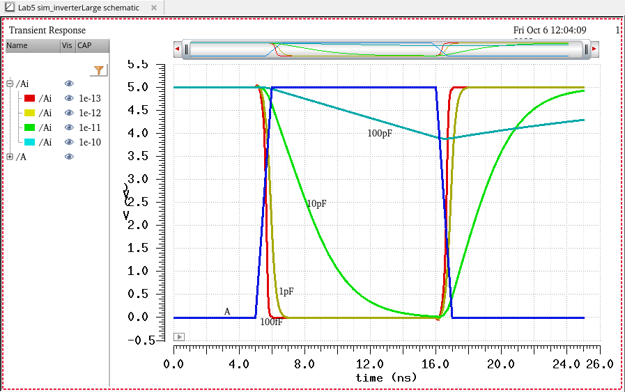
UltraSim:
Click here for Lab5 zip file.
Back-up:
Return to Index