Lab 4 - EE 421L
Authored
by Cody Woolf woolfc@unlv.nevada.edu
Today's
date: 27Sep2023
Pre-Lab:
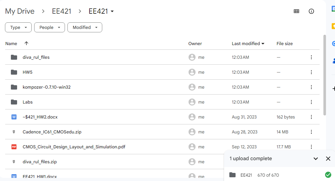
First, I backed up all my lab and course work to Google drive.
Next,
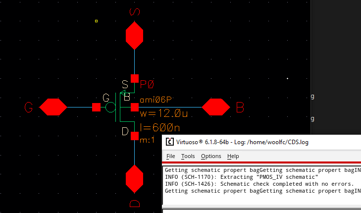
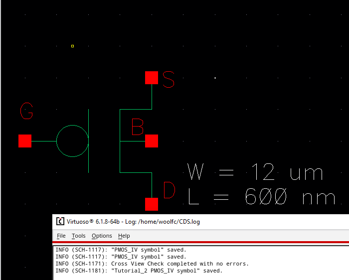
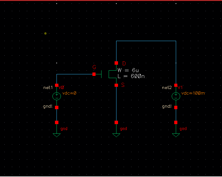
a NMOS was generated in Tutorial 2. Provided below will be the
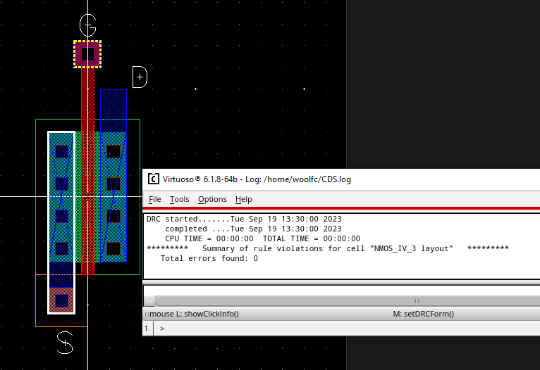
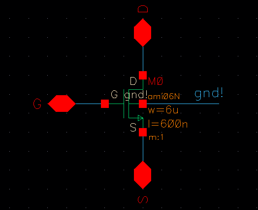
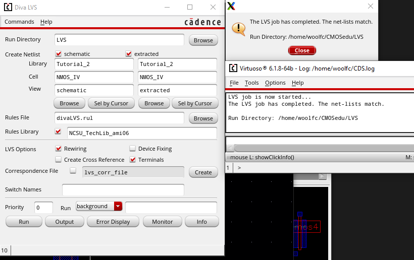
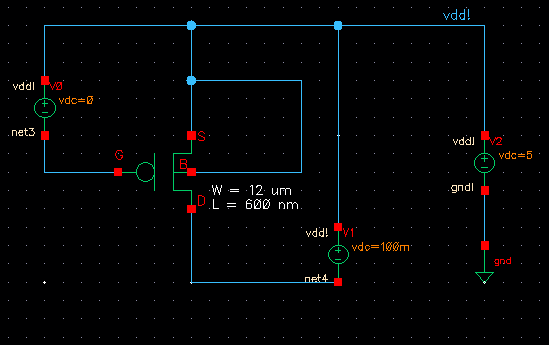
schematic of a NMOS, the symbol, simulation, layout, and the LVS.
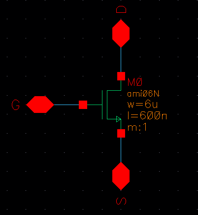
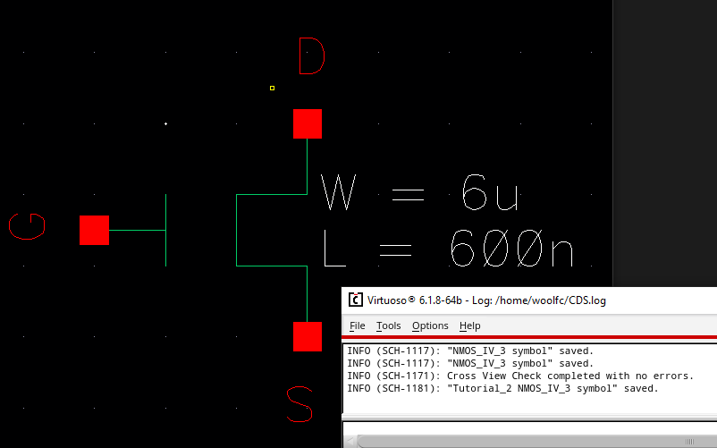
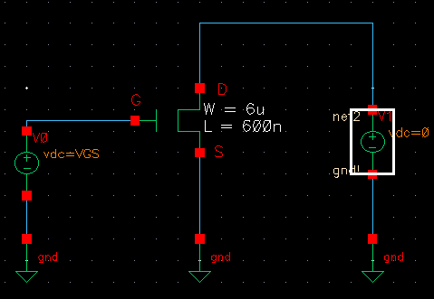
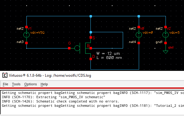
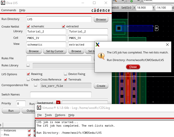
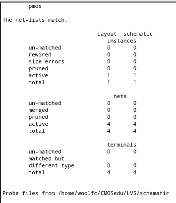
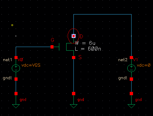
In order to LVS properly, the schematic had to be altered as seen below.
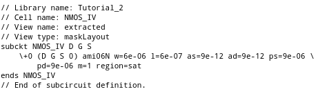
The process was repeated for PMOS.
________________________________________________________________________________________________________________________________________________________________________________
Lab
description:
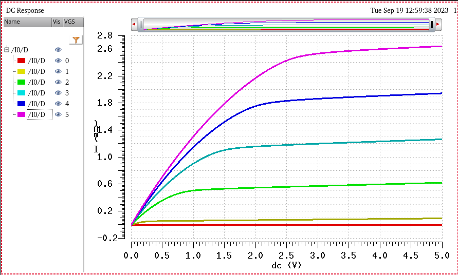
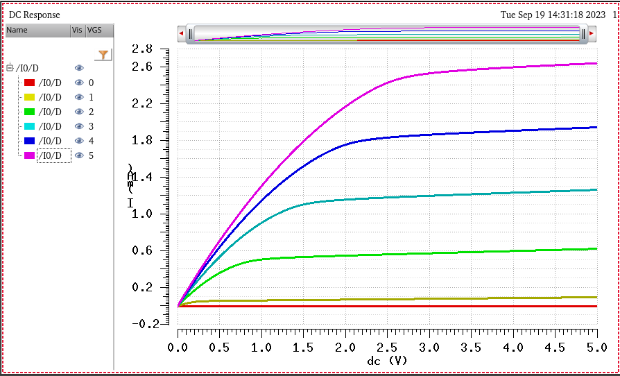
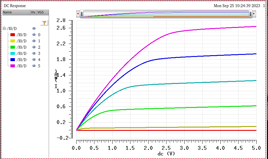
NMOS ID vs VDS (6u/600n // VGS: 0V to 5V in 1V steps ; VDS: 0V to 5V in 1mV steps):
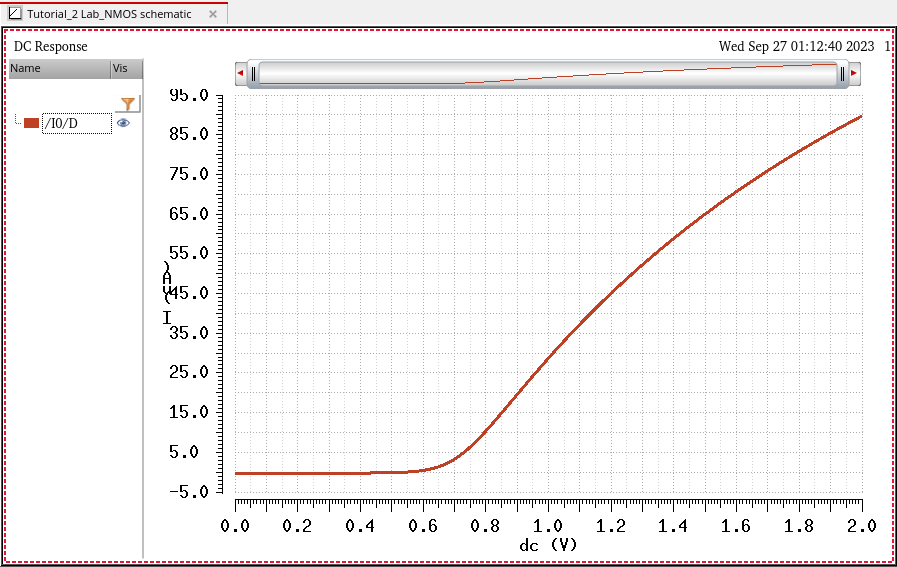
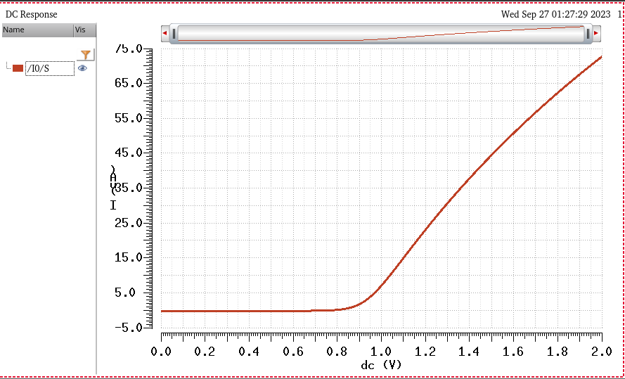
NMOS ID vs VGS (6u/600n // VGS: 0V to 2V in 1mV steps // VDS = 100mV):
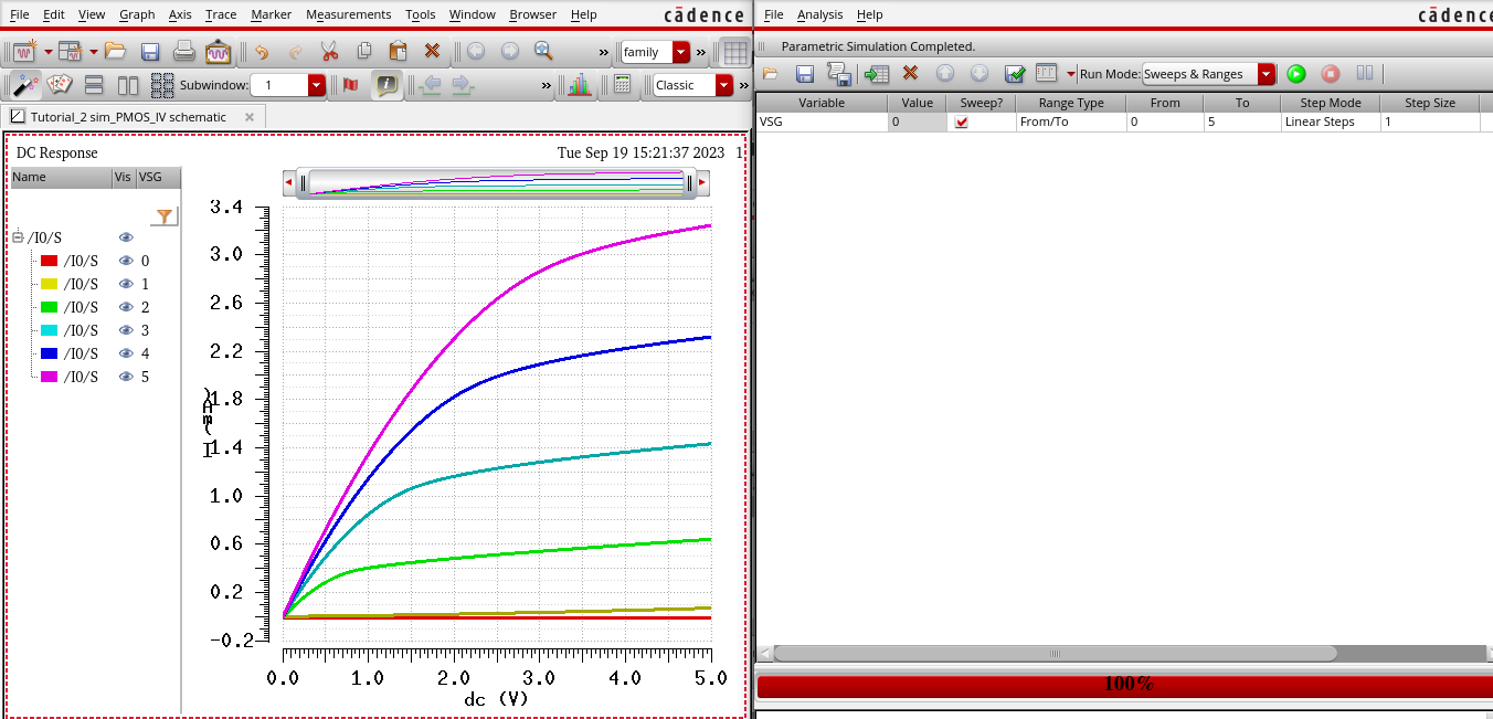
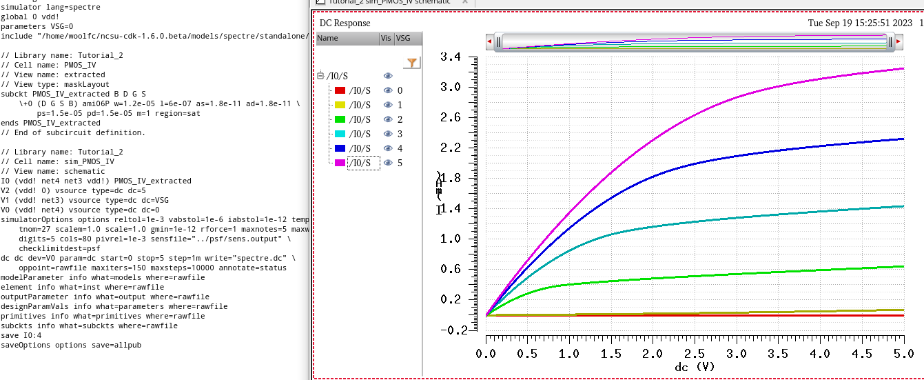
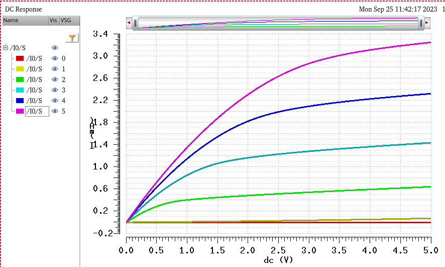
PMOS ID vs VSD (12u/600n // VSG: 0V to 5V in 1V steps ; VSD: 0V to 5V in 1mV steps):
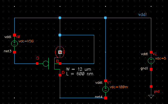
PMOS ID vs VSG (12u/600n // VSG: 0V to 2V in 1mV steps // VSD = 100mV):
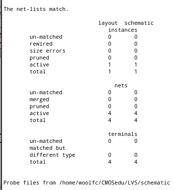
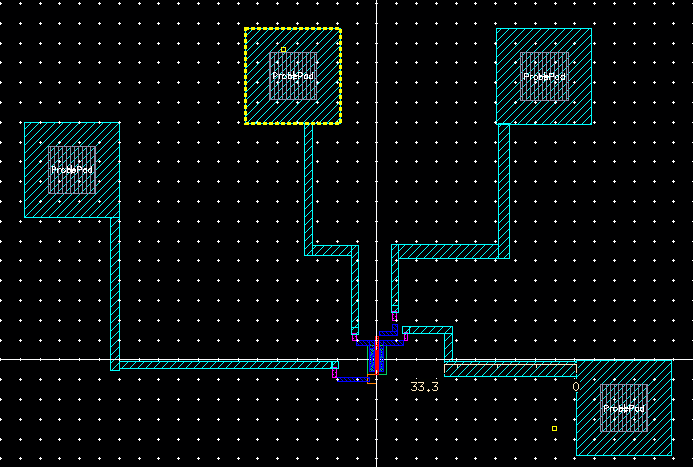
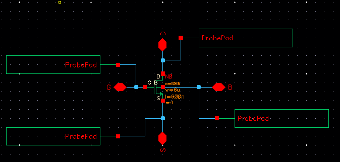
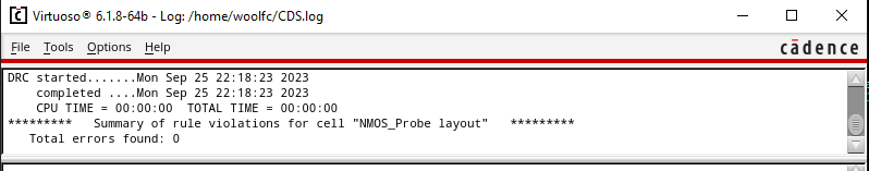
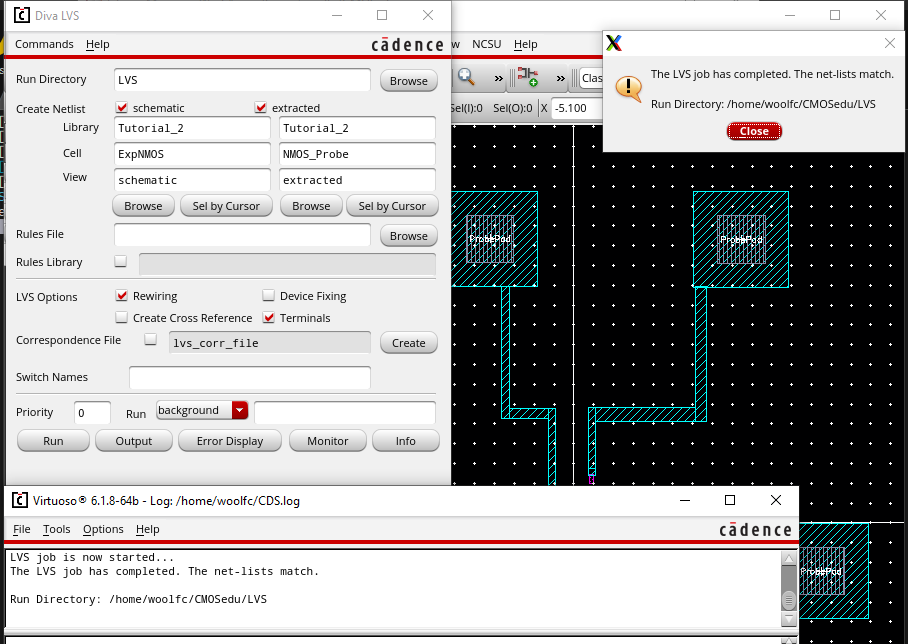
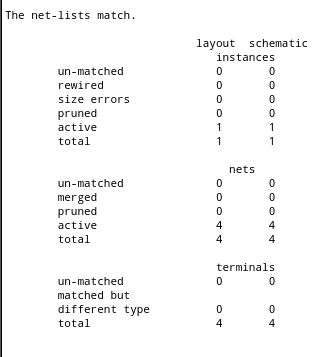
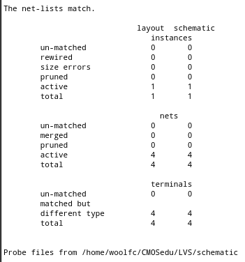
NMOS with 4 Probe Pads (Layout ; Schematic; DRC; LVS):
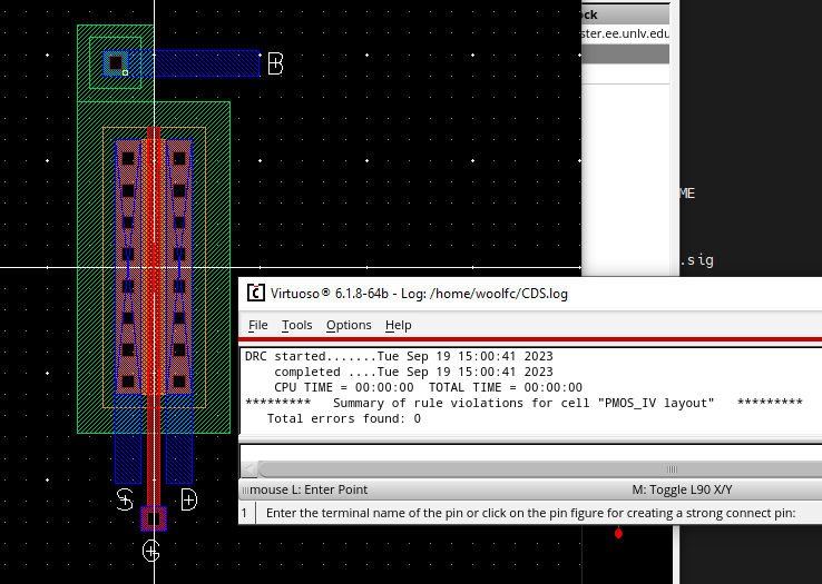
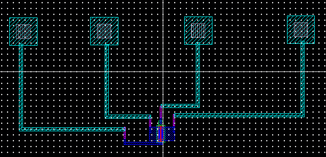
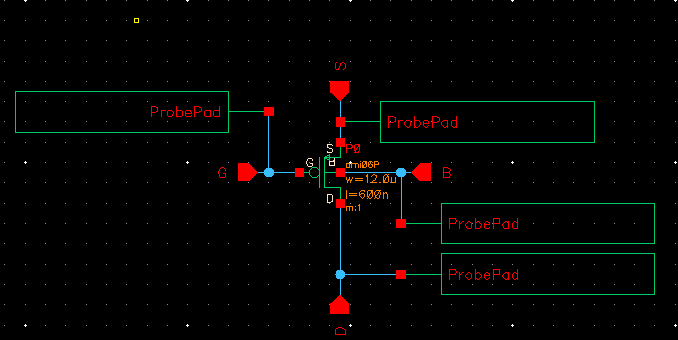
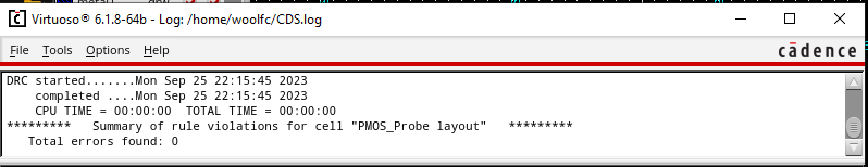
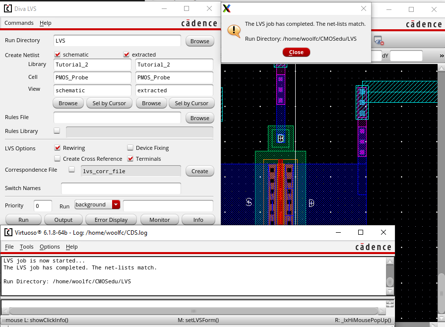
PMOS with 4 Probe Pads (Layout ; Schematic; DRC; LVS):
Backup: The backup in the Pre-Lab was updated on Google drive as seen here.
Return to Index