Lab 2 - EE 421L
Authored
by Cody Woolf woolfc@unlv.nevada.edu
Today's
date 04Sep2023
Design of a 10-bit digital-to-analog converter (DAC)
Pre Lab:
The
prelab begins with downloading the lab2 zip file. Next, it is uploaded
into CMOSedu in the remote terminal at which point it is unzipped.
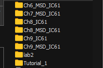
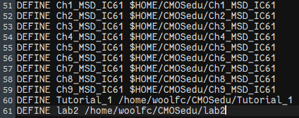
Now, it is verified that the cds.lib has the proper definition for Cadence to access lab2.
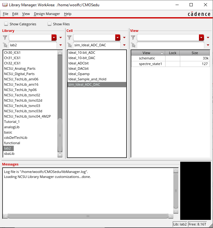
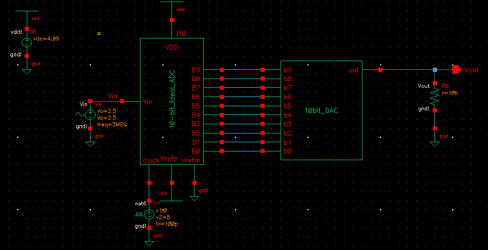
After launching Cadence, select lab2 -> sim_Ideal_ADC_DAC and access schematic.
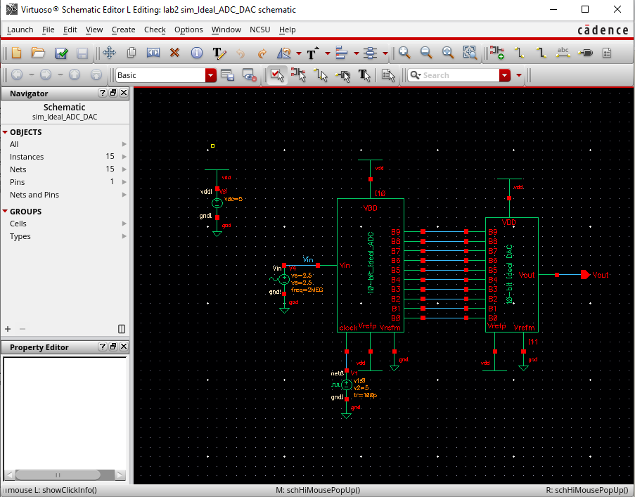
Launch in ADE L and load state.
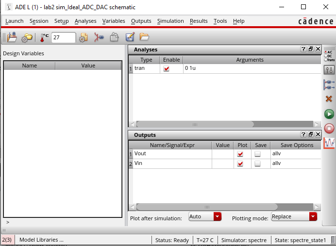
Run simulation and obtain results.
The
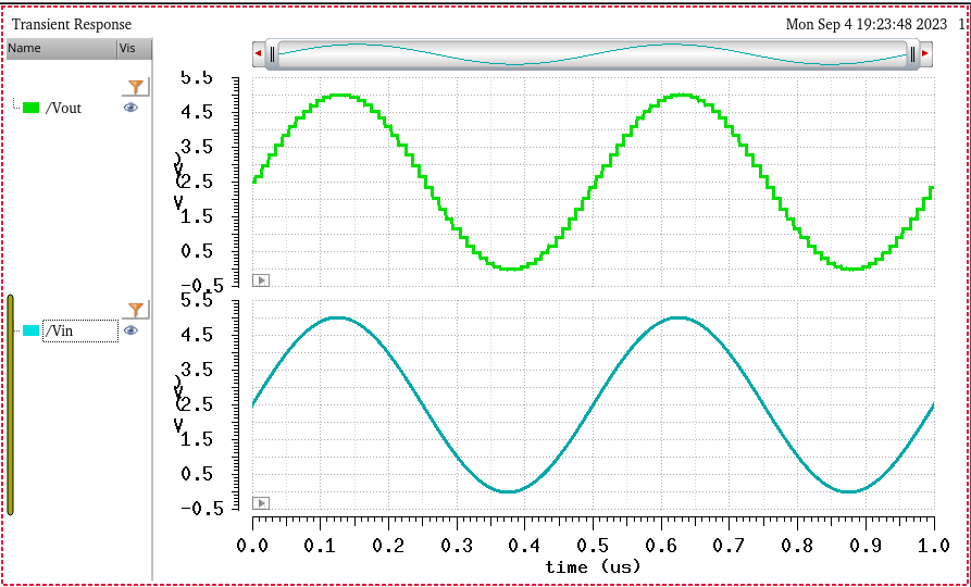
prelab then asks how Vin is related to B[9:0] and Vout. Each bit is the
input to a voltage divider. Then, by using superposition, Vout can be
extrapolated. This will give an equation that is the sum of
b9*(Vdd/(2^1)) + b8*(Vdd/(2^2)) + b7*(Vdd/(2^3)) ... + b0*(Vdd/(2^10)).
___________________________________________________________________________________________________________________________
Lab Description:
In
this lab, we used n-well resistors set at a value of 10kOhms to design
and implement a 10 bit DAC. The design was based on the following image.
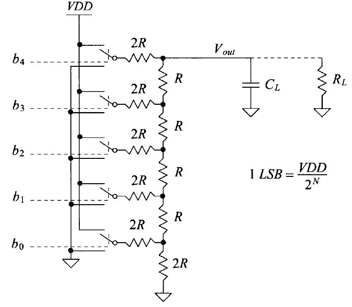
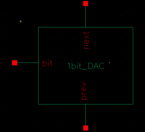
The first step was to develop a voltage divider to act as the 1 bit component.
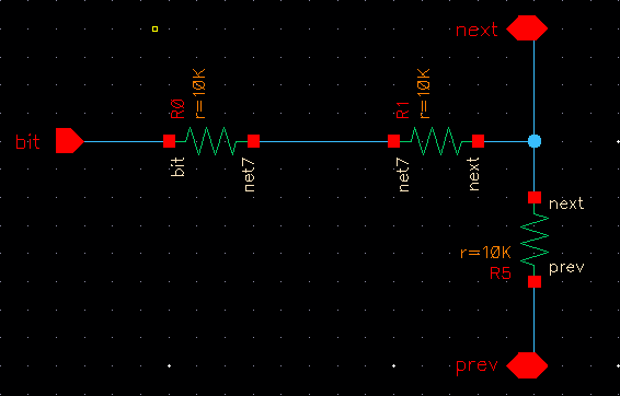
Next, a symbol was created from the voltage divider schematic.
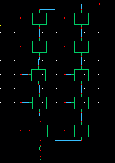
Utilizing the created symbol, a schematic for the 10 bit DAC was created.
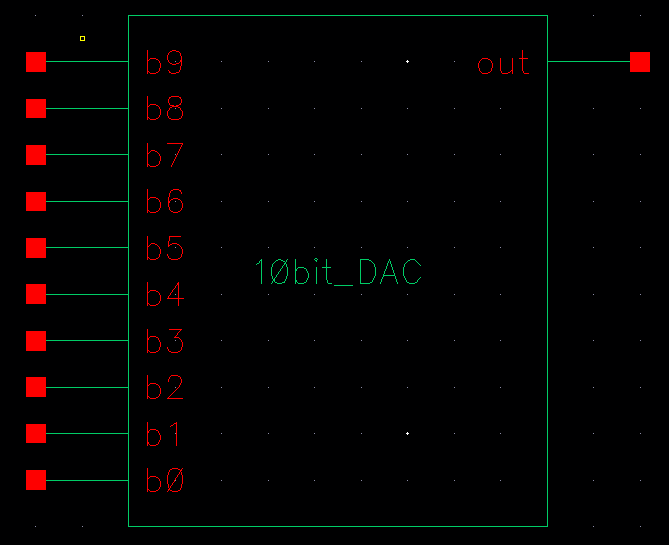
Next,
a symbol was created from this schematic. This will allow for ease of
use when making modifications to the circuit while leaving the DAC
unchanged.
Hand calculations are performed in order to determine the output resistance of the DAC.
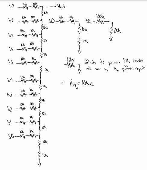
Here Req is the output resistance.
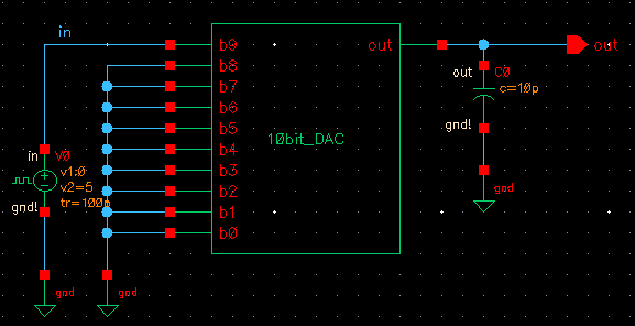
Delay:
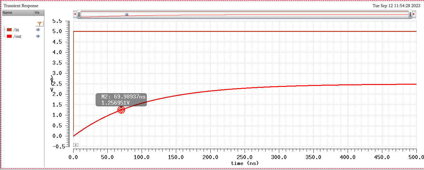
In
this step, we predict using hand calculations the delay of the DAC
driving a capacitive load of 10pF. It is then verified by grounding all
but b9 and simulating. A pulse from 0 to Vdd (5V) was connected to b9.
td = 0.7*R*C
td = 0.7*10k*10p
td = 70ns
The
expected output response is a maximum of 2.5 volts; this is determined
by 5*(1/2). At the delay, it is expected that the voltage is half of
that; that being 1.25 volts.
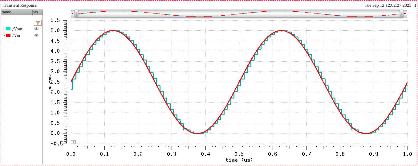
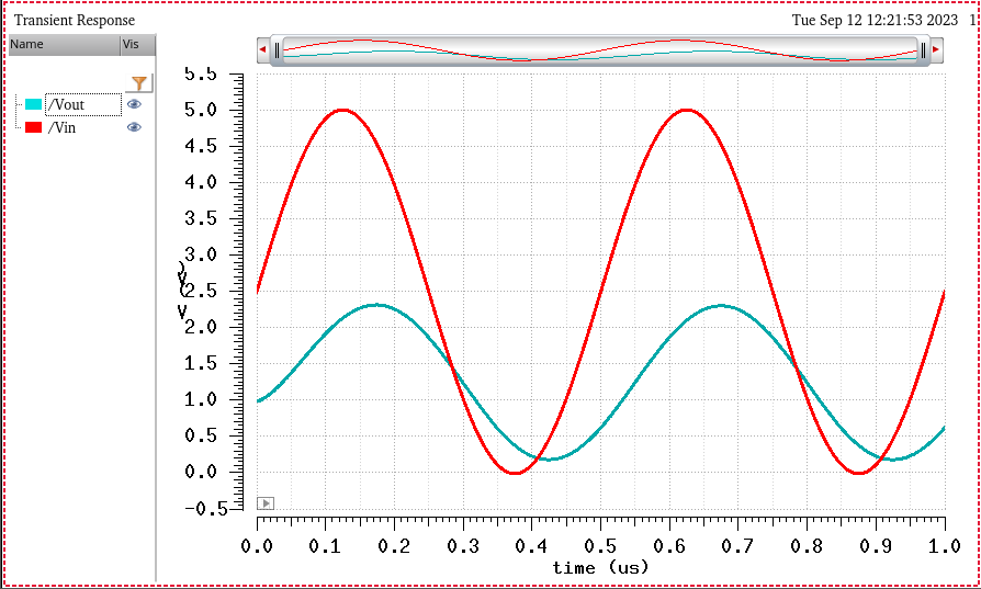
Next,
the DAC designed above is tested for validity by replacing the DAC in
the ideal ADC_DAC circuit provided to us in the lab2 zip. It is then
simulated under no load conditions.
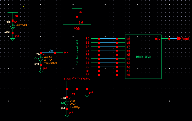
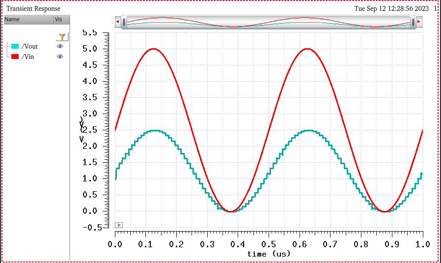
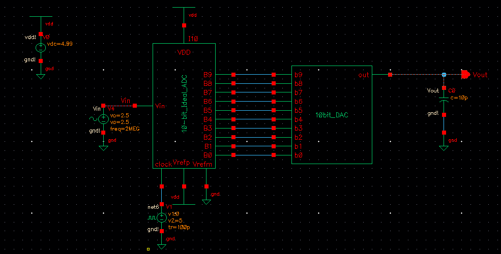
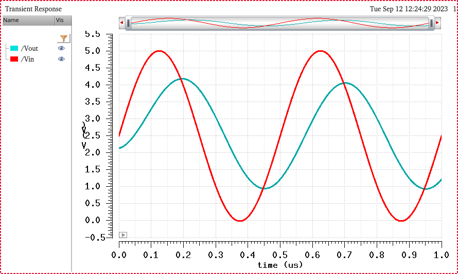
Now
that the designed DAC has been verified to operate correctly, it is
tested under three separate load conditions. First is with a 10k
resistor, second is a 10pF capacitor, and last is the two in parallel.
R Load:
C Load:
RC Load: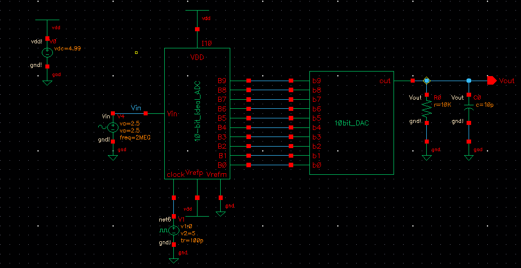
When the load is solely a resistor, we can see that the magnitude
is halved. When the load is solely capacitive, we can see that the
magnitude of the output is the same but the wave is delayed. When the
load is the two in parallel, the magnitude is halved and the wave is
delayed.
If the circuit was real, the switches
(outputs of ADC) are implemented by MOSFETs. Therefore, if the
resistance of the switches is not small in comparison, then this
creates another resistance in series for the voltage divider. This then
lowers the output voltage.
Return to index.