Final Project - ECE 421L
Project (NOT a group effort) – design a non-inverting buffer circuit that presents less than 100 fF input capacitance to
on-chip logic and that can drive up to a 1 pF load with output voltages greater than 7V (an output logic 0 is near ground
and an output logic 1 is greater than 7V). Assume VDD is between 4.5V and 5.5V, a valid input logic 0 is 1V or less, a valid
input logic 1 is 3V or more. Show that your design works with varying load capacitance from 0 to 1 pF. Assume the slowest
transition time allowed is 4 ns.
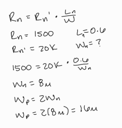
First, I calculated the size of the first inverter based off of a resistance value I chose, which was 1.5k. The calculations are as follows:
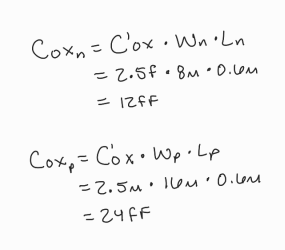
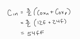
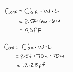
After I calculated the size of the transistors in the inverter, I next verified those sizes would meet the design requirement of the input capacitance being less than 100fF. Those calculations are as follows:
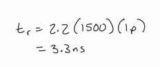
Next, I verified that the sizes would meet the delay requirement of being less than 4ns, and that calculation is below:
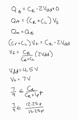
The last set of calculations I did was to calculate the size of MOSFETs to be used as capacitors, as later when we layout the schematic, that will be a better alternative. The first capacitor that will be connected to node A needed to be very small, and the capacitor connected to node B needed to be larger than our load capacitance. A few different sizes were tried until I settled on the sizes shown in the calculations below:
Next I verify the size of the "capacitor" over the inverter on the right is sized approriately with the following calculation:
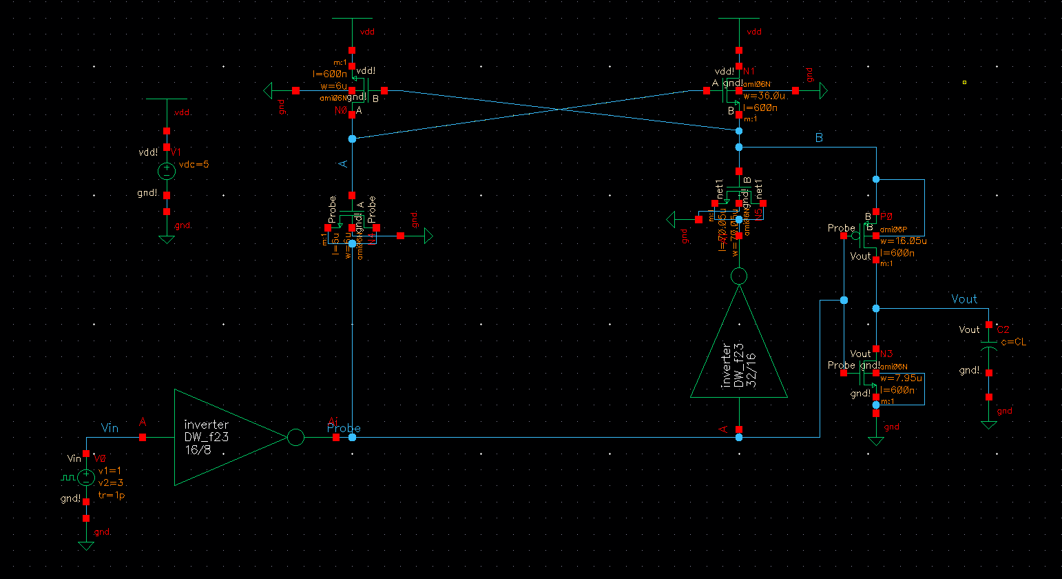
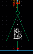
After calculating all the sizes I would use for within the circuit, I then assembled the circuit and it looks like this:
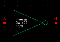
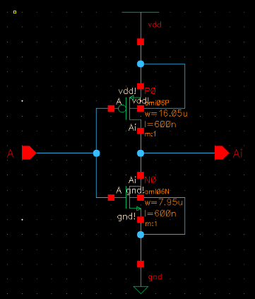
The size and schematic of the first inverter are as follows:
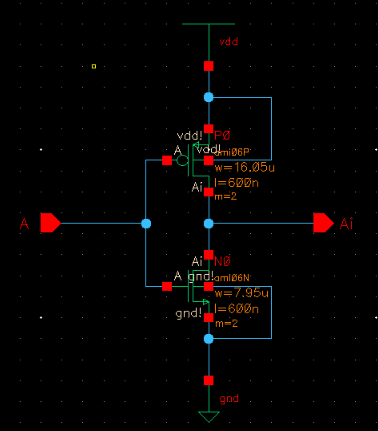
The size and schematic of the second inverter are as follows:
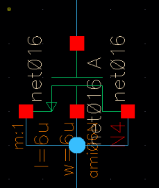
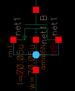
A close up of the "capacitor" connected to node A is as follows:
A close up of the "capacitor" connected to node B is as follows:
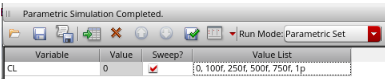
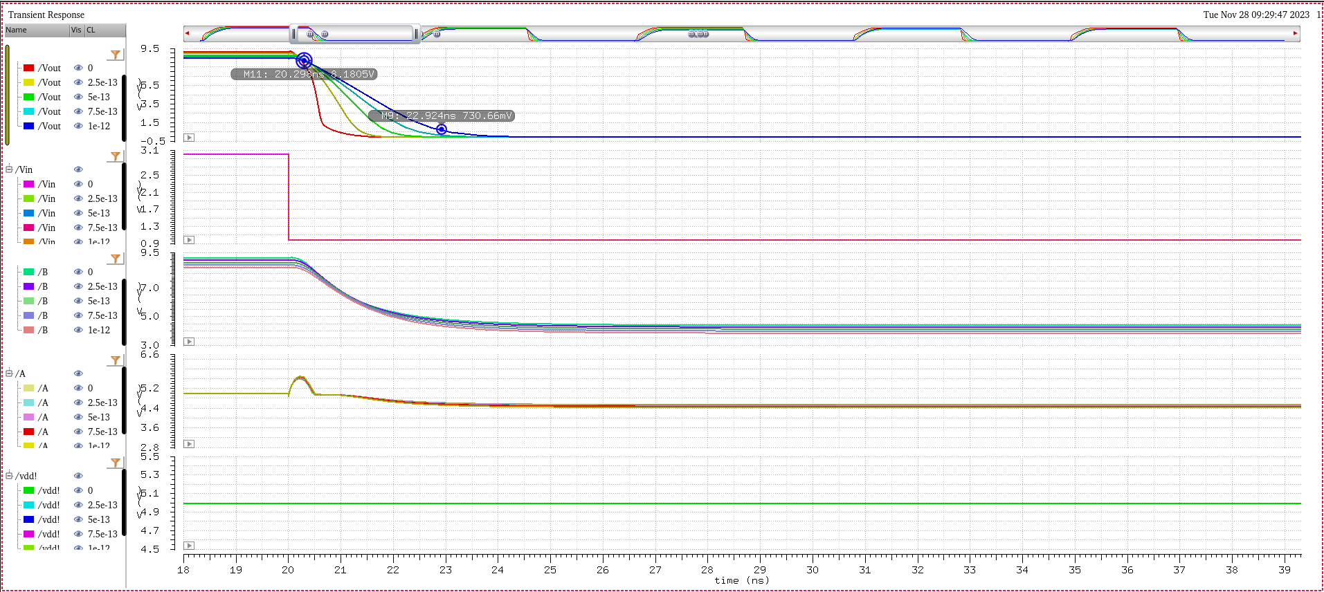
Once the circuit was fully assembled, I ran a parametric analysis so that I could test the circuit under varying capacitive loads. The loads are as follows:
These
loads produce the following waveforms, as you can see, node B produces
an output that is approximately twice the value of VDD, which is what
we expect to happen:
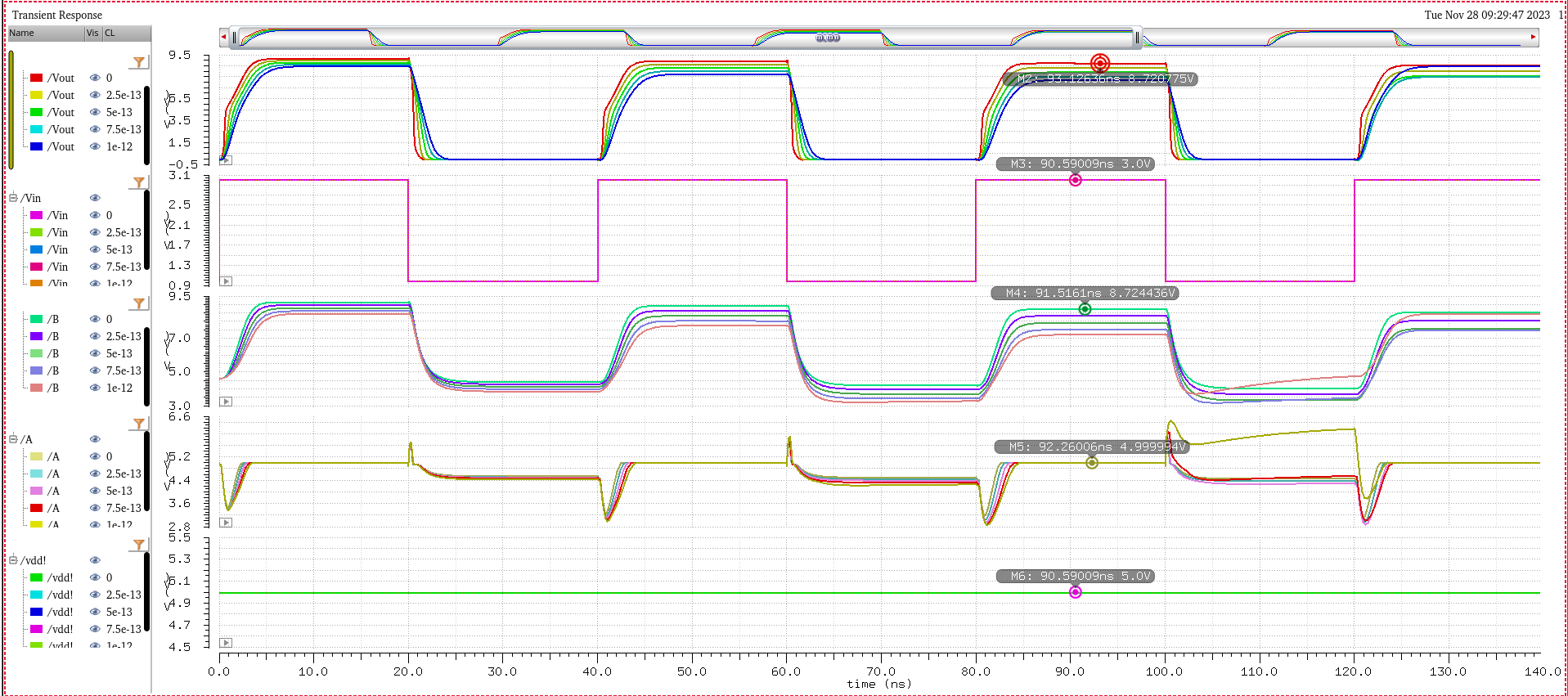
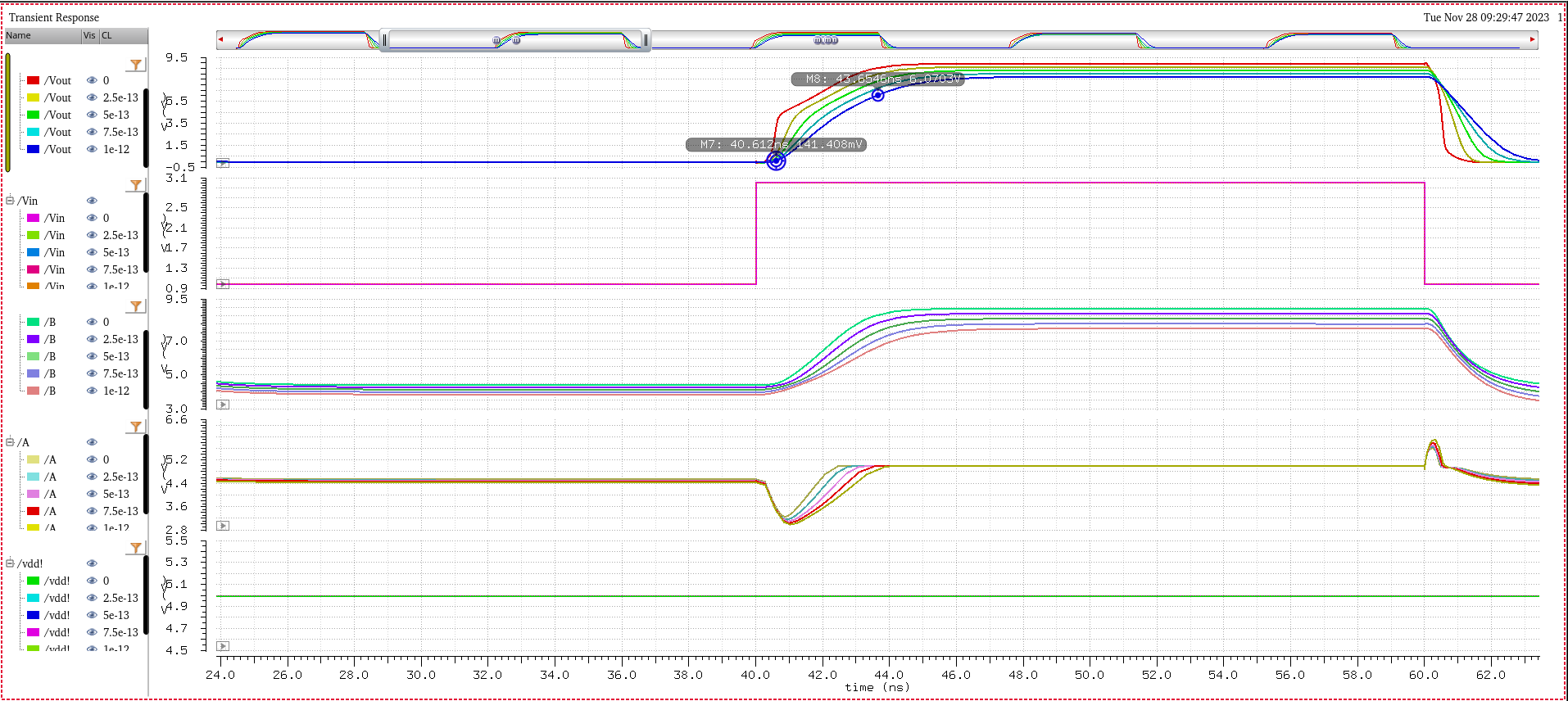
Next, we verify the delay:
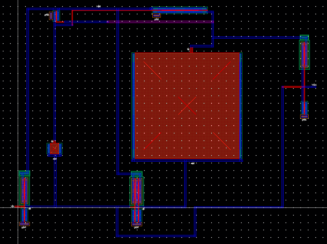
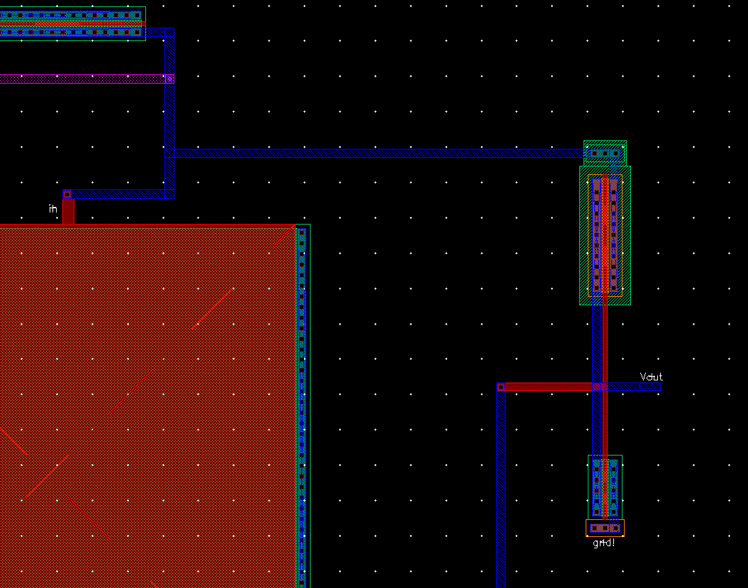
Next I built the layout for the Non-Inverting Buffer Circuit and it is the following:
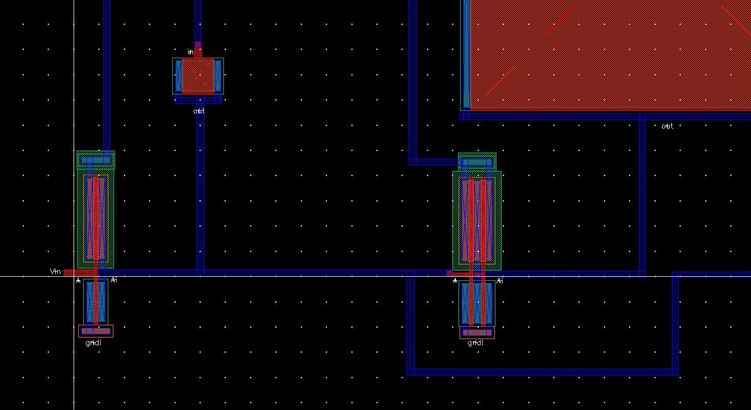
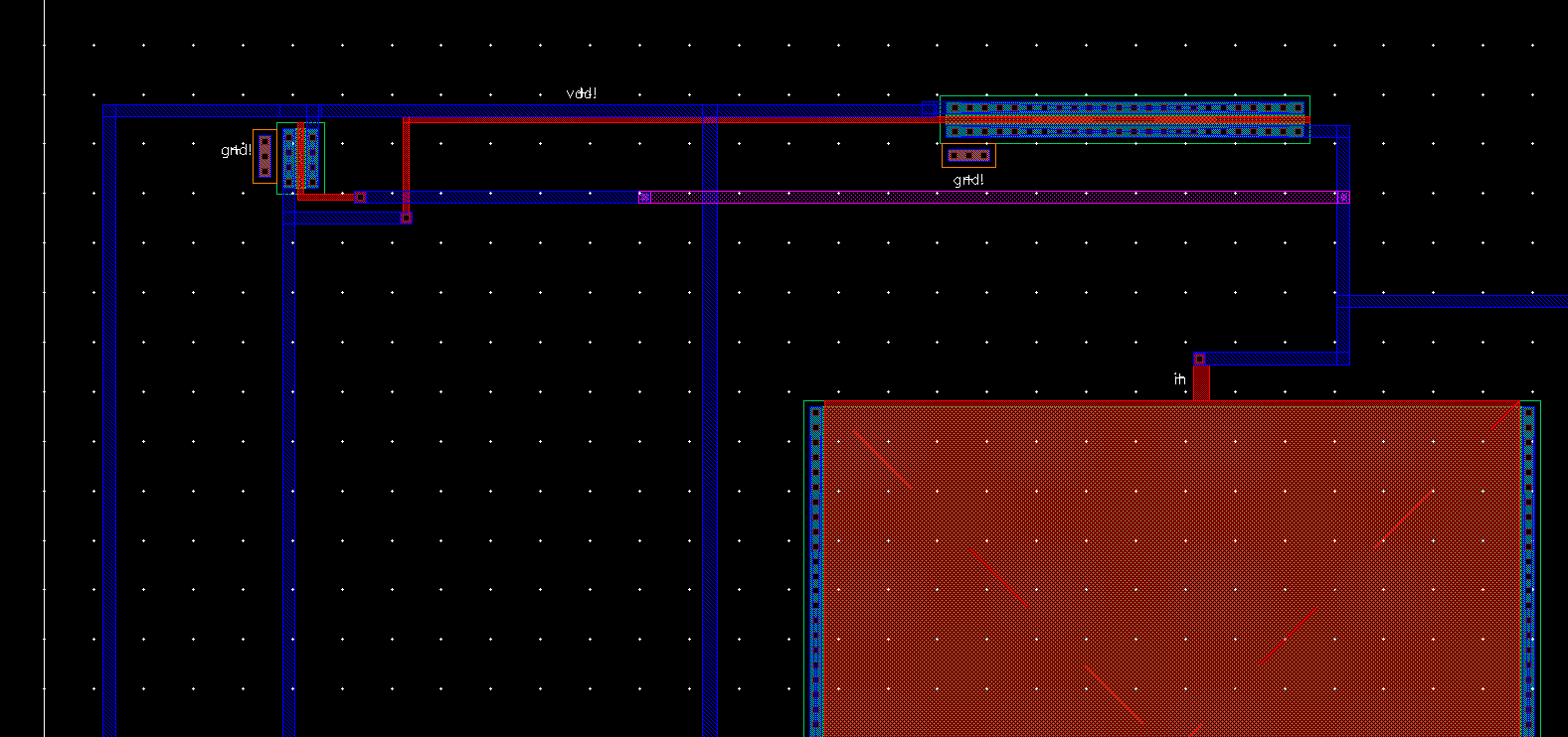
Some close ups of the different areas of the circuit are as follows:
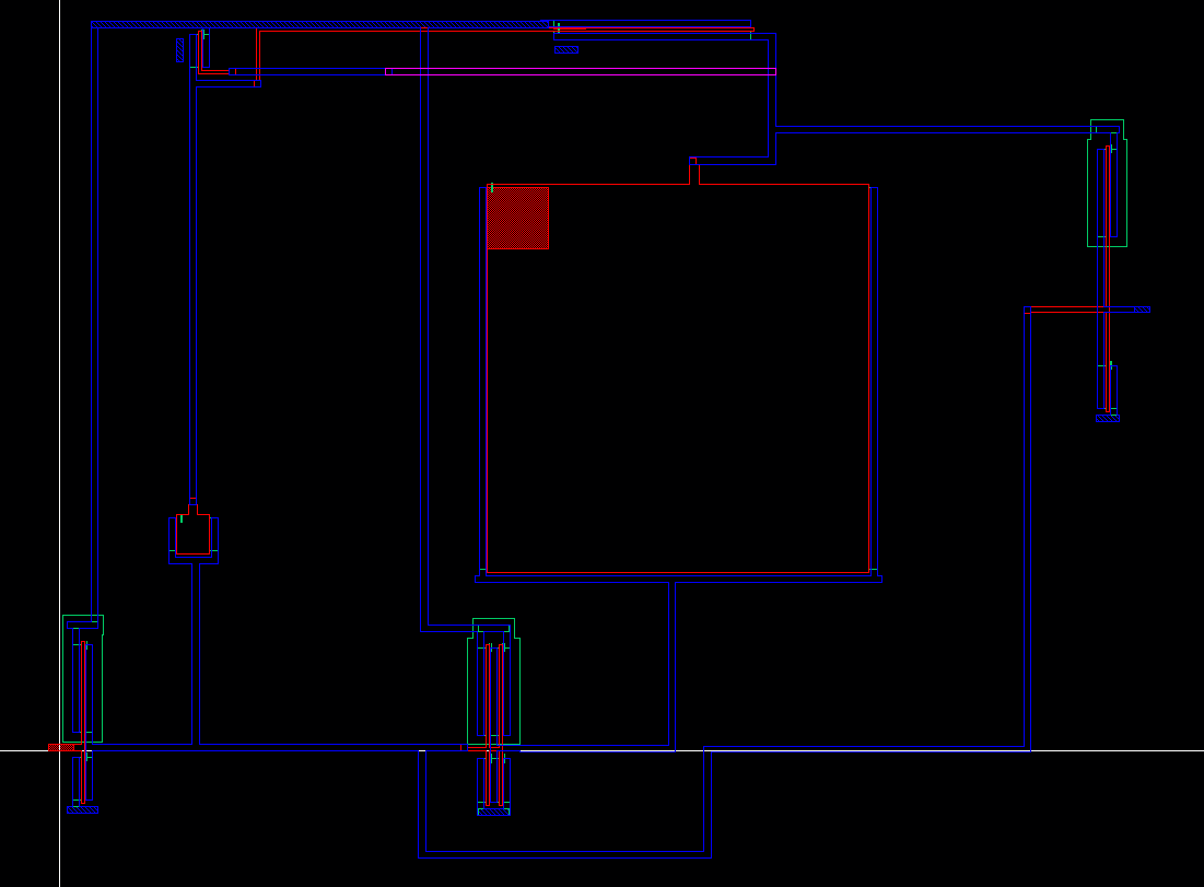
Here is the extracted view:
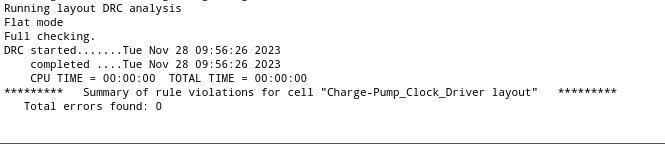
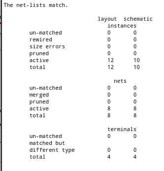
Next is proof of DRC/LVS clean:

Here is the files for the project.
Return to labs