Lab 8 - ECE 421L
Authored
by Edgar Rodriguez Nevares, Dara Wells, Cody Woolf
Rodrie27@unlv.nevada.edu
Wellsd5@unlv.nevada.edu
Woolfc@unlv.nevada.edu
12/06/2023
Backup:
Creating a backup for Lab 8 by downloading the zip file
Lab Purpose:
While
working a group of three we are tasked to fabricate an integrated chip
by placing the previously created schematics and layouts onto a pad
structure.
Pre-lab:
1.) Go through the beginning of Tutorial 6.
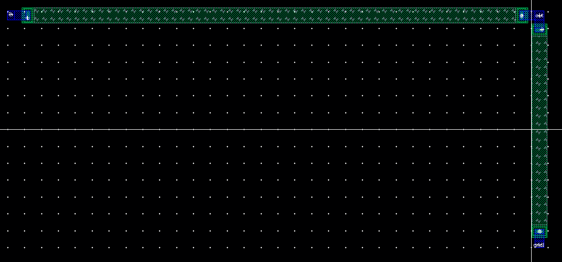
Initial metal and pad with glass:
Single pin with pad:
40 pins around exterior:
LAB 8: Generating a test chip layout for submission to MOSIS for fabricationThe
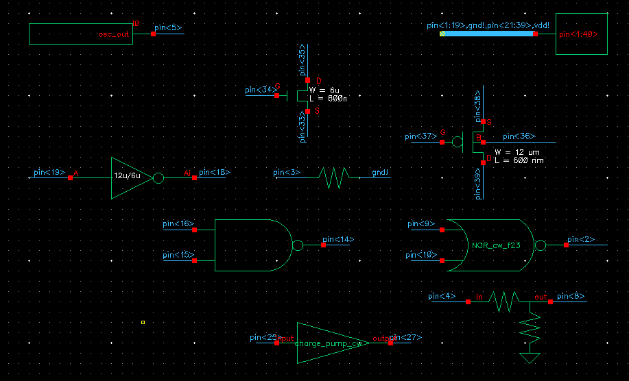
first step of lab 8 is to create an 31-ring oscillator: which is an
array of odd number inverters that acts as a buffer between the input
and output signal.
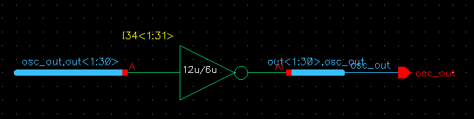
After composing the schematic we created the layout for the ring oscillator.
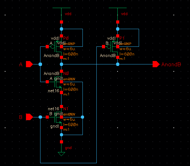
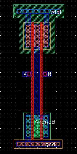
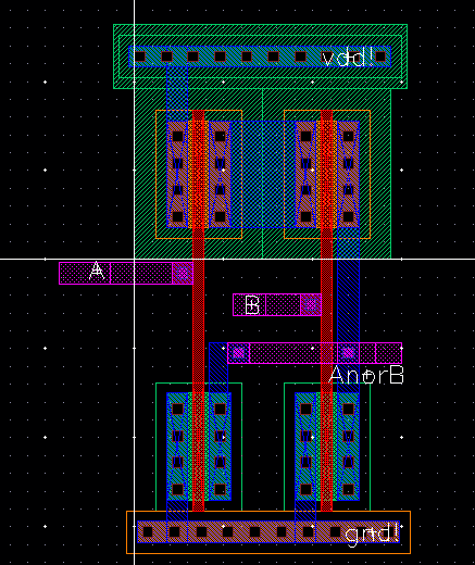
After the ring oscillator the next step was to create the schematic and layout for the two-input NAND gate.
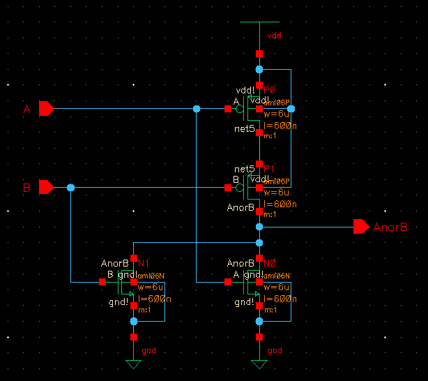
From there we moved onto creating the layout of a two-input NOR gate.
The next step in the lab was to create a 12u/6u MOSFET schematic and layout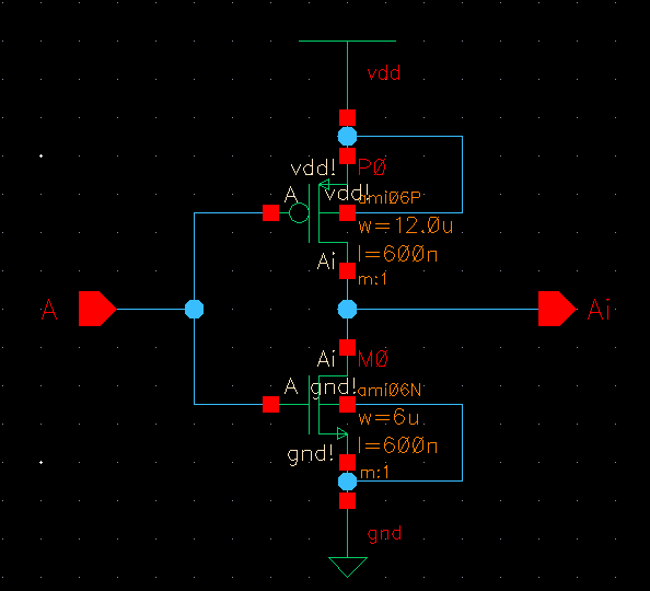
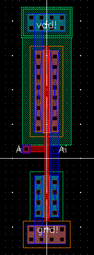
Once done with the MOSFET we moved onto crafting a 6u/600n PMOS transistor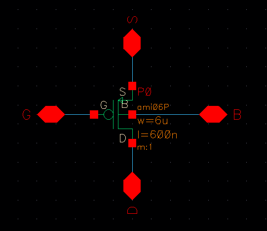
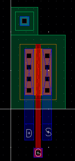
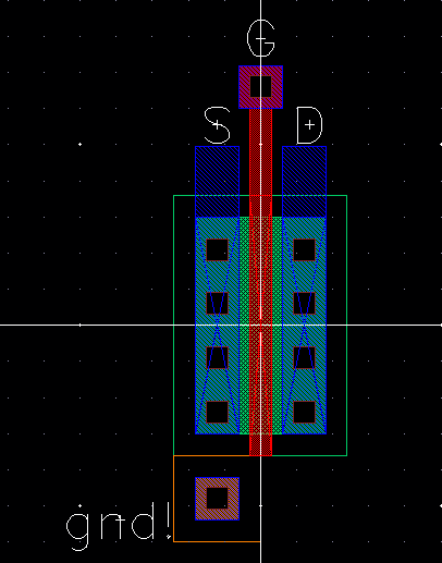
Once done with PMOS we created a 6u/600n NMOS schematic and layout. 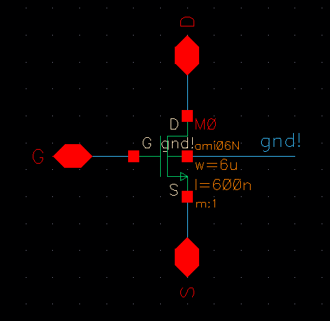
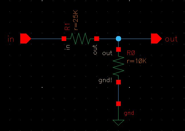
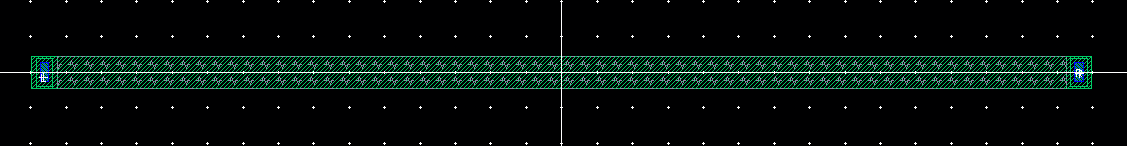
From crafting the MOSFETs we moved onto creating a voltage divider schematic and layout to be placed onto the pad.
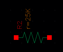
The last step before running simulations on our created cells was to create a 52k ohm resistor schematic and layout.
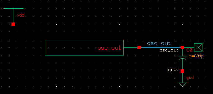
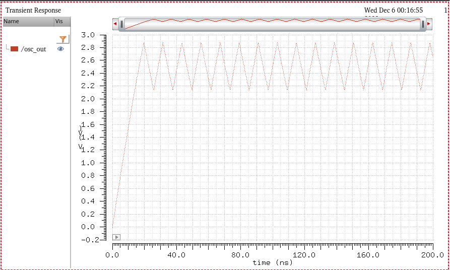
After crafting the 52k ohm resistor; the next step was to simulate the ring oscillator with a 20pF capacitive load.
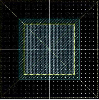
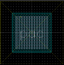
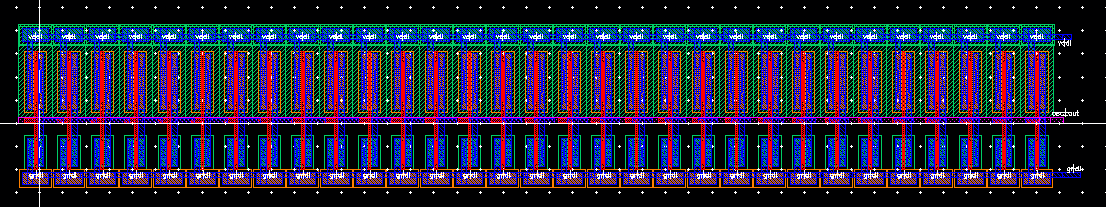
Here we place the cells into one giant schematic cell that will be placed onto a the fabricated chip pad.
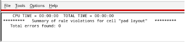
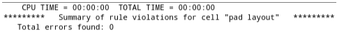
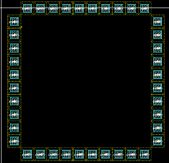
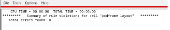
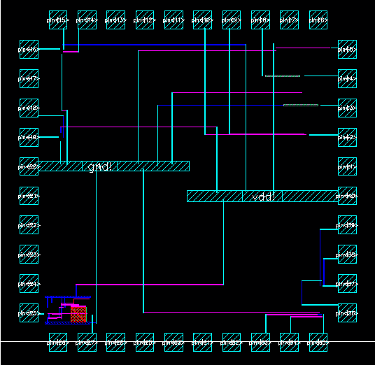
Once the schematic form for our lab was created we then created the pathing for the cells onto the pad created in tutorial 6.
With this our lab is concluded.
Our lab files can be downloaded here.
Edgar Rodriguez Nevares' Labs
Dara Wells' Labs
Cody Woolf's Labs