Lab 6 - ECE 421L
Authored
by Dara Wells, wellsd5@unlv.nevada.edu
10/21/2023
Design, layout, and simulation of a CMOS NAND gate, XOR gate, and Full-Adder
Prelab:
The prelab has students go through Tutorial 4. Tutorial 4 had students design, layout, and simulate a NAND gate.
This is the schematic for the NAND gate:
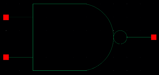
Next we created a symbol for the NAND:
Next we created a circuit to test the function of our NAND seen in the following:
Next, we created a layout of the NAND and ran LVS to make sure it is clean:
Lab:
This lab has students design, layout, and simulate a NAND gate, XOR gate and a Full-Adder.
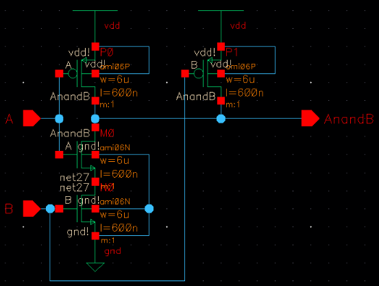
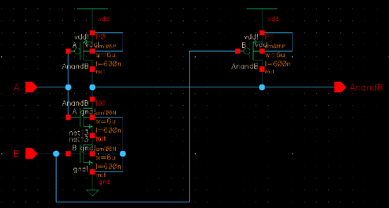
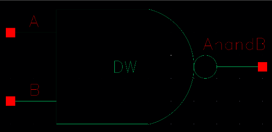
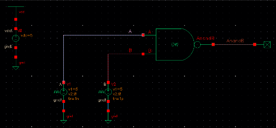
First
we have the schematic and symbol for the NAND, which is very similar to
the one used in the tutorial, but with some minor changes:
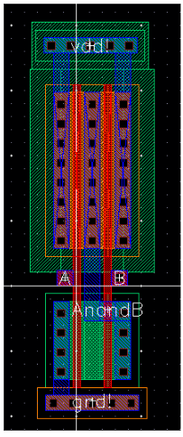
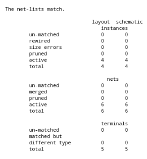
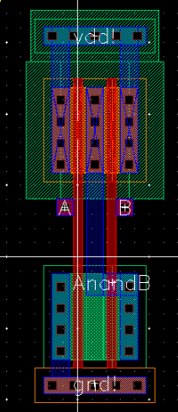
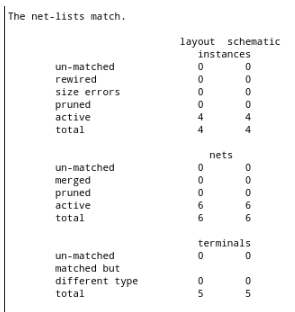
Next, we created the layout and ran it through LVS:
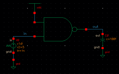
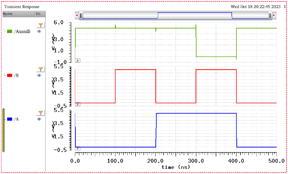
Next,
we want to see that our NAND functions correctly so we run it through a
basic two-bit logic sequence to see what the simulations look like. We
use the symbol to create a circuit and the simulations can be seen as
follows:
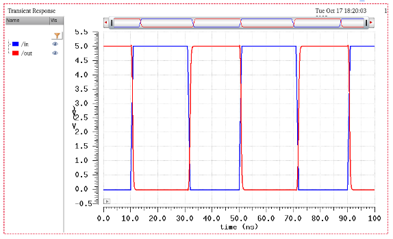
On the sim we see some glitches, so to smooth them out we add some inverters and the simulations then look as follows:
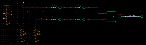
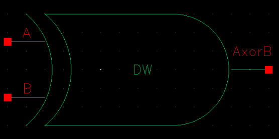
Second, we design, layout, and simulate a XOR gate. The schematic and symbol are as follows:
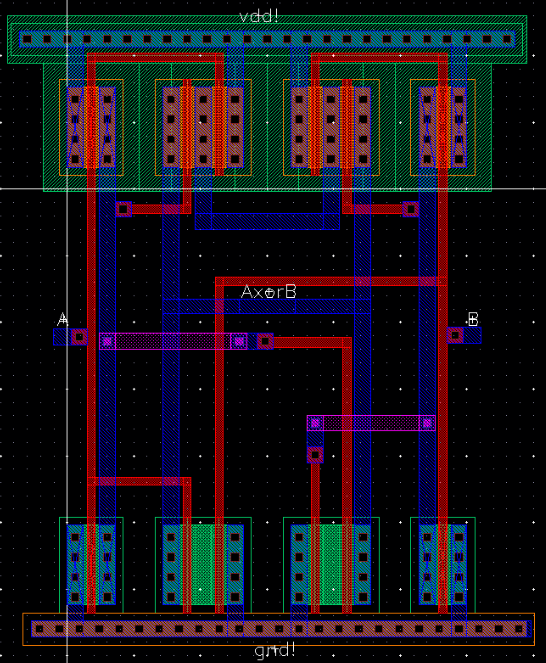
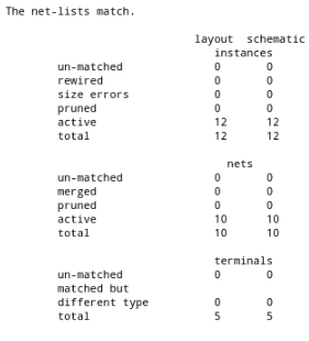
Next we created the layout and checked to see that it is LVS clean:
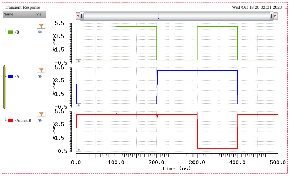
Then
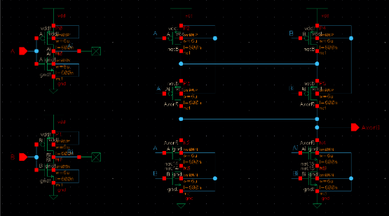
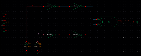
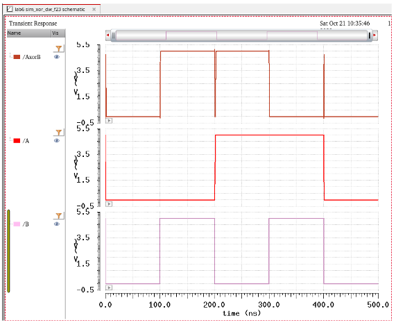
we used the XOR gate in a ciruit to verify its logic outputs, using
inverters again to minimize any glitching in the simulations:
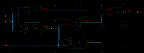
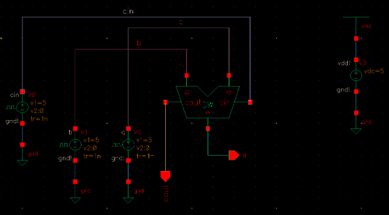
Lastly
we used our NAND and XOR to create a Full-Adder, first using the
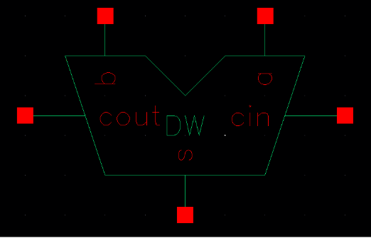
symbols to create the schematic, then making a symbol for the
Full-Adder:
Next, we make a layout for the Full-Adder, using the layouts we made for the XOR and NAND:
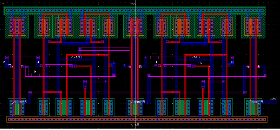
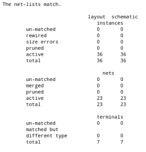
Then we make sure the layout is LVS clean:
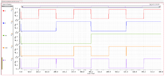
Now
that we have the Full-Adder, we want to use it in a circuit so we can
verify the nature of the outputs are as they should be expected:
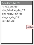
Here is verification of proper labeling of the cells:
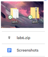
Here is proof of my backup of the lab:
Return to labs.