Lab 2 - ECE 421L
Design of a 10-bit digital-to-analog converter (DAC)
Pre Lab:
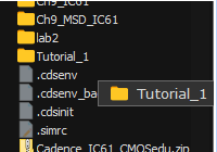
The Pre lab has us first download and upload a zip file to our directory on CMOSedu then unzip it:
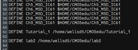
Next we defined the directory to be accessed within Cadence:
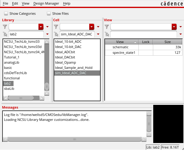
After that we loaded the schematic into Cadence by doing the following:
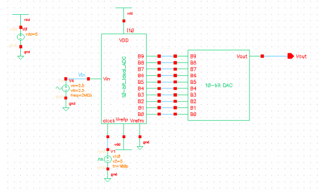
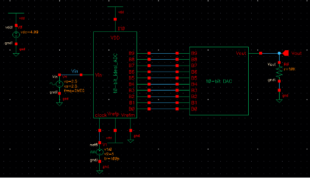
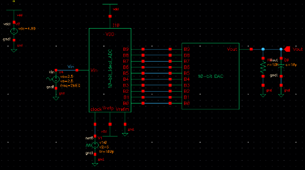
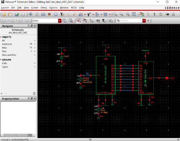
Next we viewed the schematic for the ADC DAC:
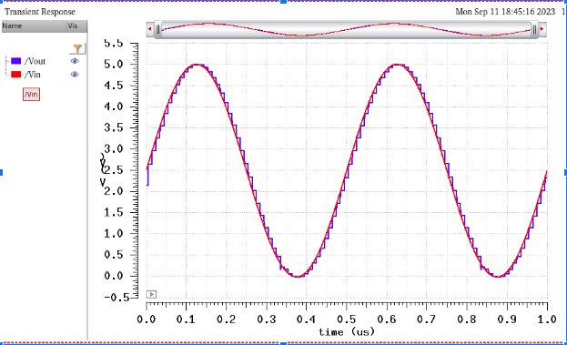
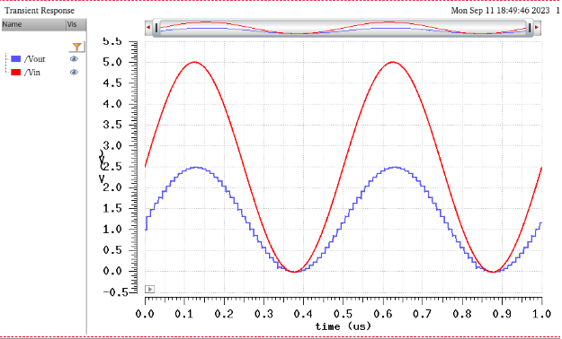
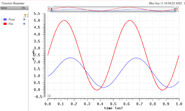
After that we plot Vin and Vout to see the waveforms:
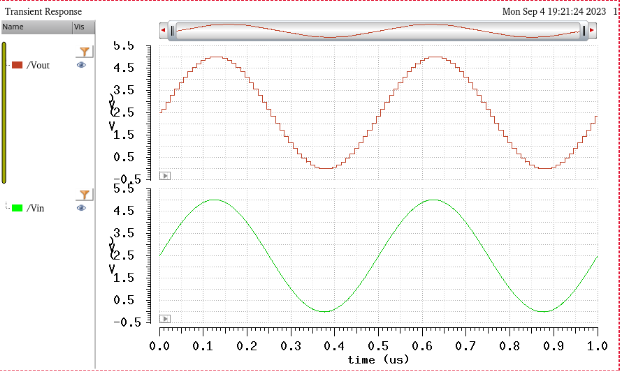
The prelab then asked to know the relationship between Vin and B[9:0] and Vout. They are related by multiples of the LSB which in this case the LSB is determined using the equation 1 LSB = Vdd/2^n and by plugging in values is 1 LSB = 5/2^10 which is 4.88mV. Therefore, if you take the input, then see how many multiples of 4.88mV it is within a range of +/- 2.44mV, you can then see what the Vout is going to be. For example, if the input is less than 2.44mV, Vout will be 0V. If it is over 2.44mV by 1 multiple, then Vout will be 4.88mV and an additional 4.88mV for every 2.44mV increase.
______________________________________________________________________________________________________________________________
Lab:
This
lab has us use n-well resistors to create and implement a 10-bit DAC
(digital-analog-converter). The design we used is based off of the
following:
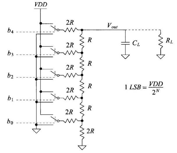
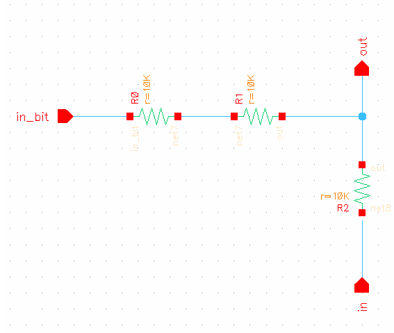
The first component we needed to create was a voltage divider for one bit.
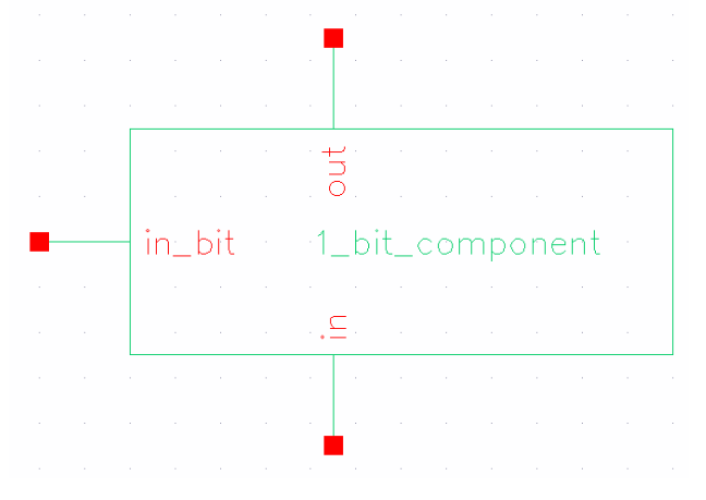
After that we needed to convert this schematic into a symbol that we can use in another schematic to replicate for all 10 bits.
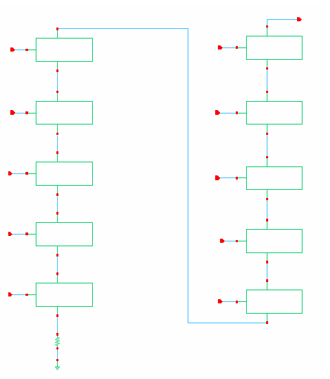
Then
we convert this schematic into a symbol as well that we can easily make
changes to the input and load for simulation and testing.
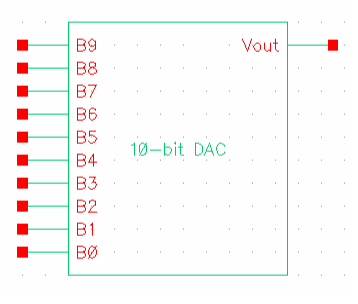
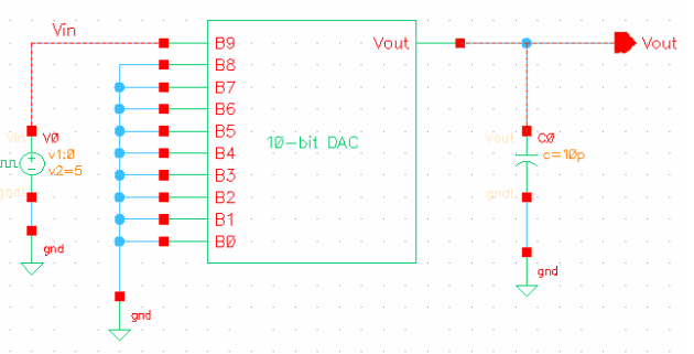
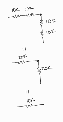
Next, we needed to determine the output resistance of the DAC which can be done as follows:
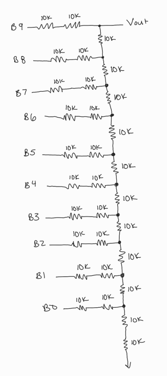
Because the equivalent resistors following the following sequence, R = 10k. This sequece repeats from bottom to top to get a total R of 10k ohms.
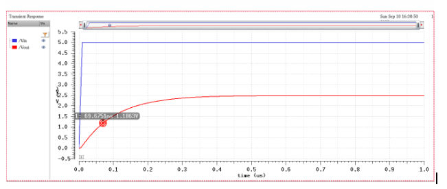
Next we had to determine the delay. This was done by grounding bits B0 - B8 and running a pulse into B9. From that we can see what the output would be. The delay is found by the following equation:
Delay = 0.7RC = 0.7(10k)(10p) = 70ns
The following is the schematic and simulation showing 70ns.