Lab 7 - ECE 421L
Authored
by Batya Vishnepolsky, vishnepo@unlv.nevada.edu
11/7/23
Lab
description
in
this lab we learn about the design of a NAND, XOR, and a full adder using those components
Prelab Description
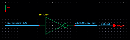
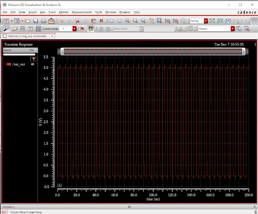
Tutorial five:
Schem:
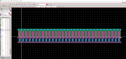
Layout:
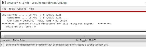
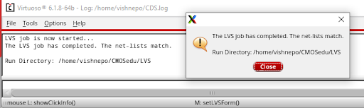
DRC and LVS:
Simulation results:
Lab work:
We went through the 4 bit inverter and 2to1 MUX and simulated them to learn about them:
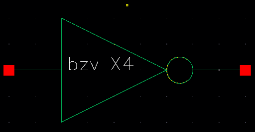
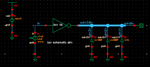
4-bit inverter:
Schem:
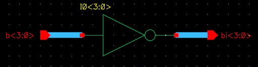
Symb:
Simulation:
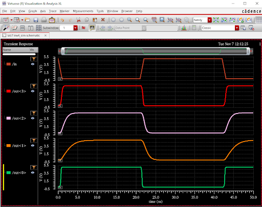
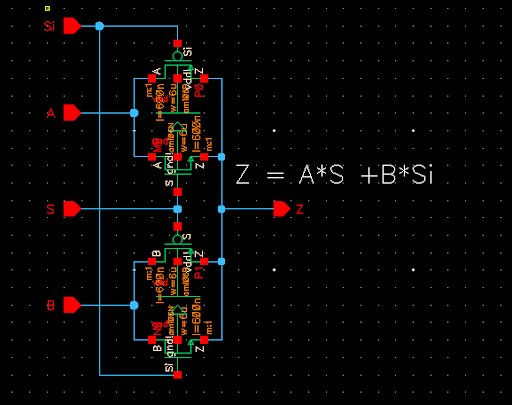
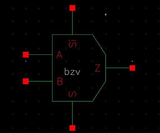
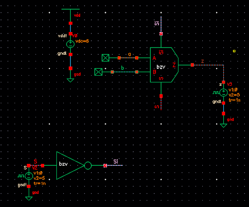
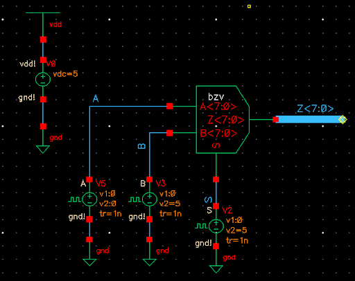
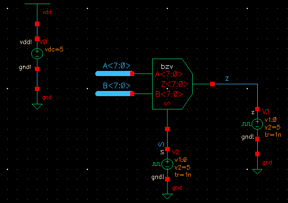
2to1 MUX:
Schem:
Symb:
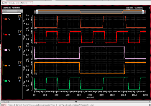
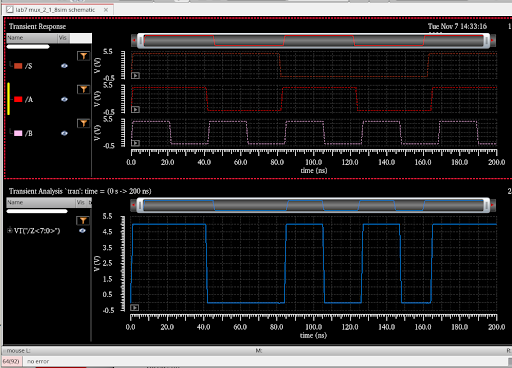
Simulation acting as a mux:
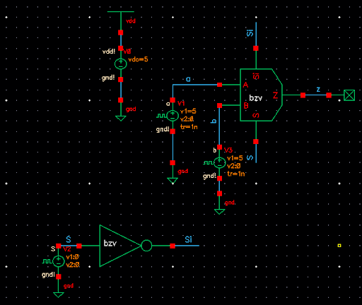
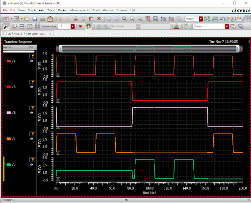
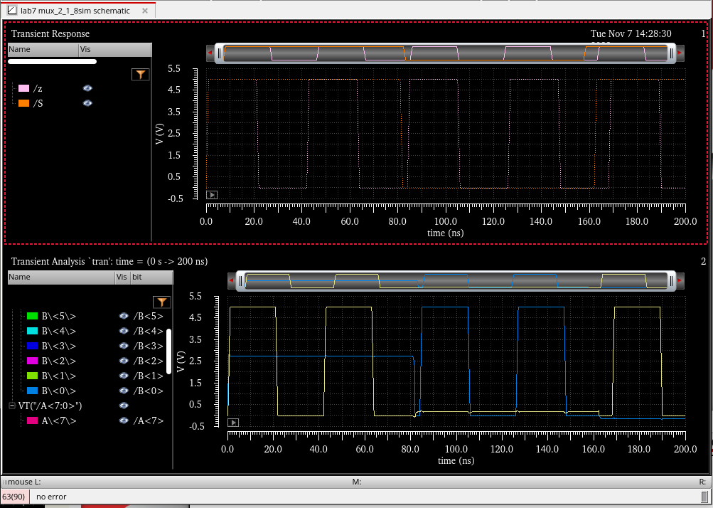
Simulation acting as a demux:
Explanation for MUX behavior:
Mux behavior:
When
the s input of the mux goes high, the z output will take the previous
A’s input. When the s input goes low (or si goes high), then the z
output thats the previous B’s input.
Demux behavior:
When s input is low, B follows the Z input. When s is high, then A follows the z.
Next I was directed to make a bunch of logic components that could handle an 8-bit input.
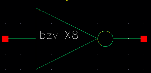
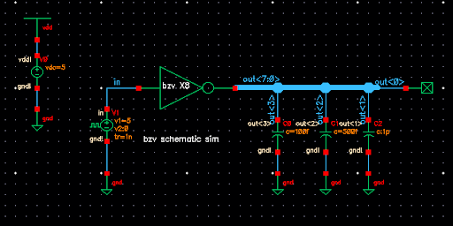
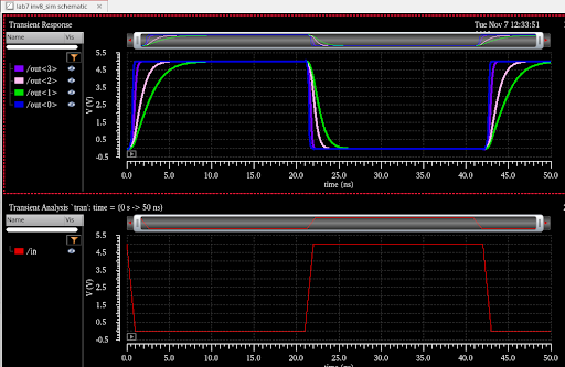
8-bit inverter:
Schem:
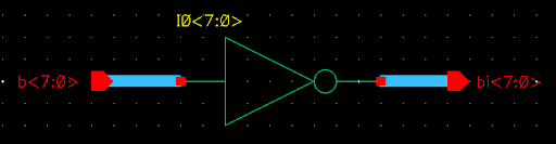
Symb:
Simulation:
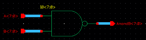
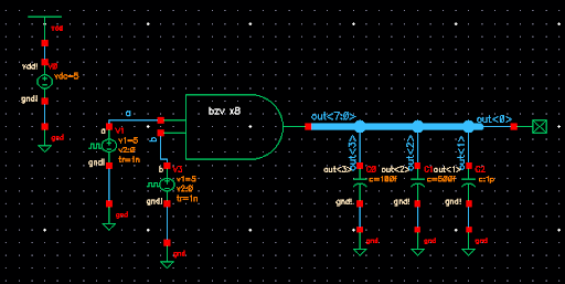
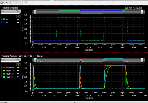
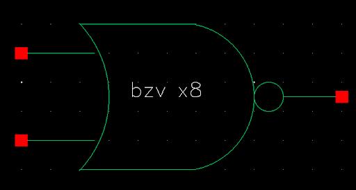
8-bit NAND:
Schem:
Symb:
Simulation:
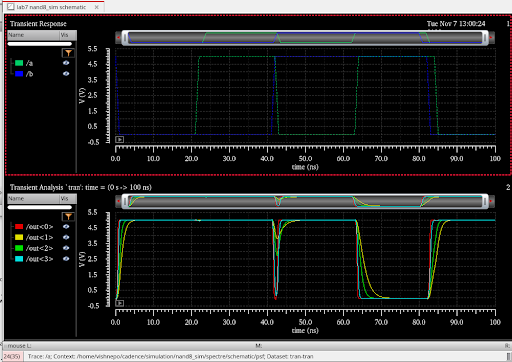
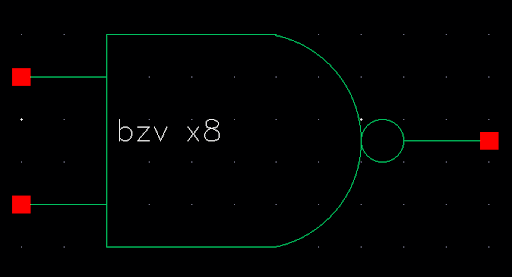
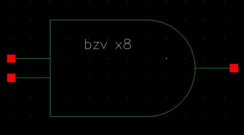
8-bit AND:
Schem:
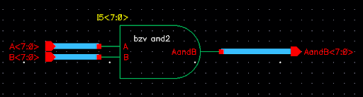
Symb:
Simulation:
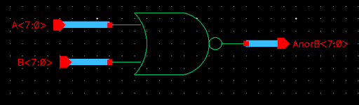
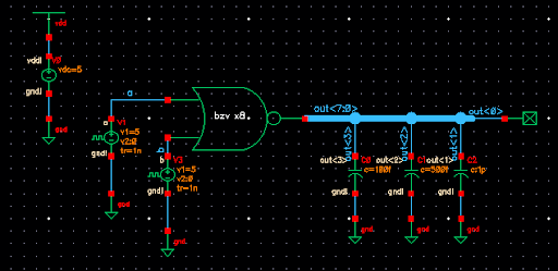
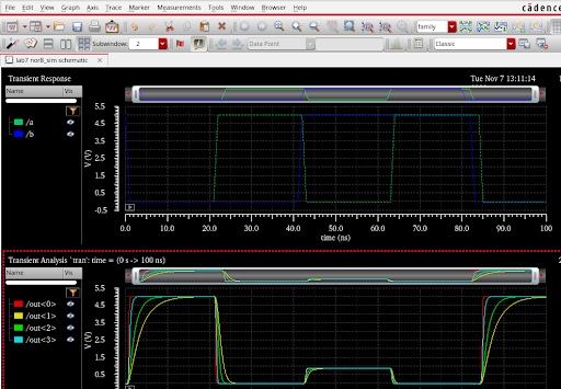
8-bit NOR:
Schem:
Symb:
Simulation:
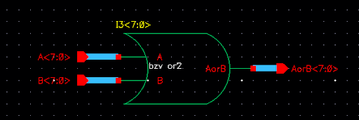
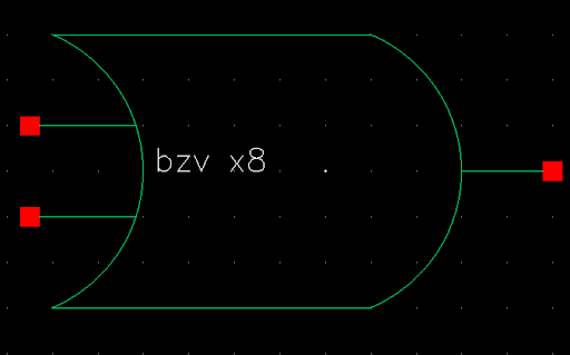
8-bit OR:
Schem:
Symb:
Simulation:
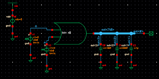
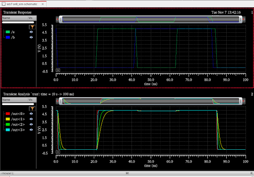
8-bit MUX:
Schem:
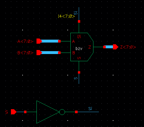
Symb:
Simulation (MUX behavior):
Simulation (de-MUX behavior):
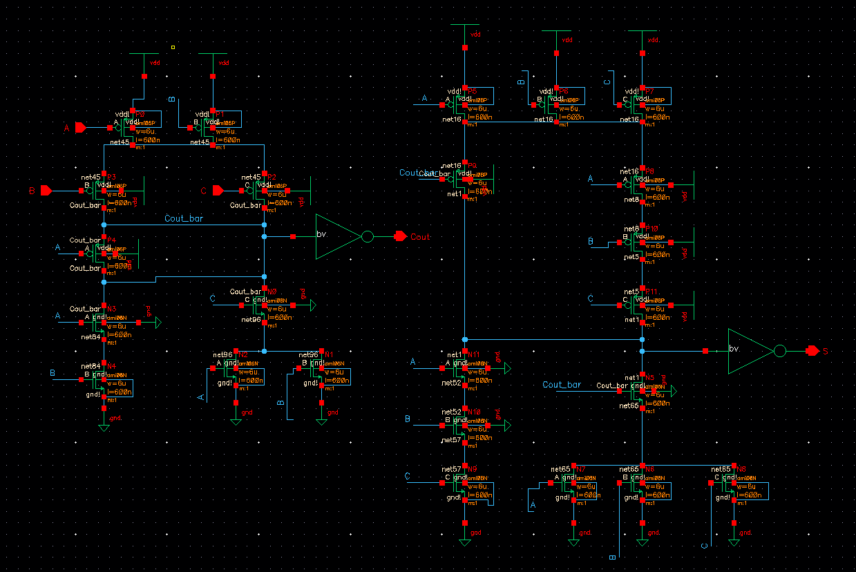
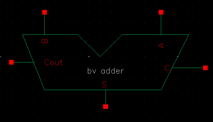
Next, I created a full adder schematic, symbol, and simulated it.
Schem:
Symb:
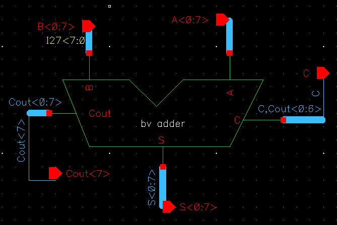
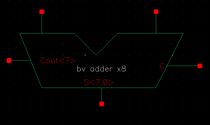
8-bit versions:
Schem:
Symb:
Return to all of Batya's Labs