Lab 5 - ECE 421L
Authored
by Batya Vishnepolsky, vishnepo@unlv.nevada.edu
10/9/23
Lab
description
In this lab we learn about the construction of a CMOS inverter.
Prelab Description
I backed up all my work from the labs as seen in previous lab reports.
I read through the lab before starting it,
And then I had to go through
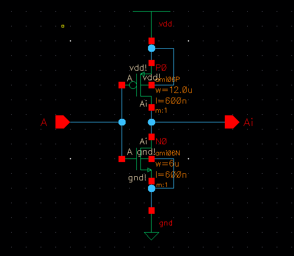
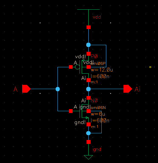
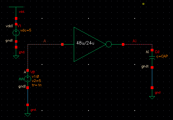
tutorial #3 on Dr. Baker's website, which walks you through the creation of an inverter created using a NMOS and
PMOS MOSFET. I generated a schematic, symbol, and layout generation. Below are a few snippits
of what I did in tutorial 3:
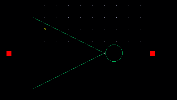
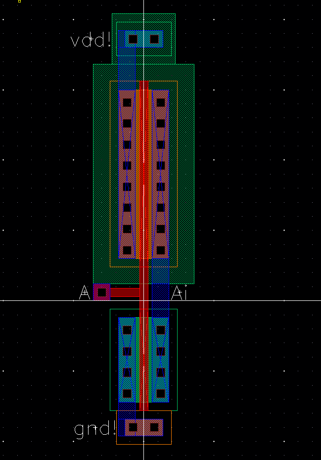
Inverter schematic, symbol, and layout:
Schem and symbol:
Layout and extraction:
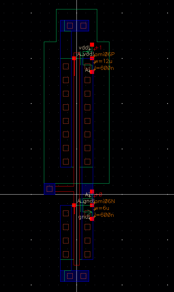
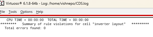
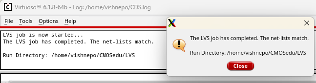
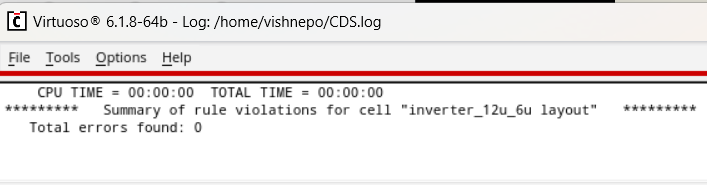
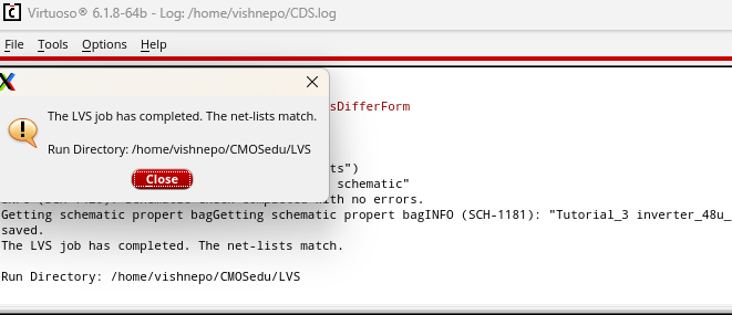
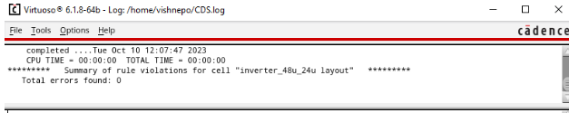
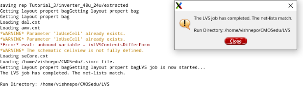
DRC and LVS:
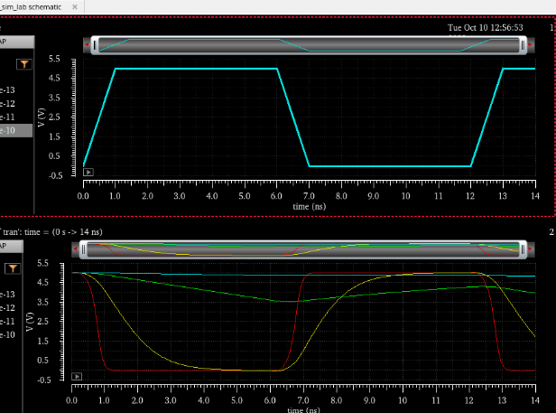
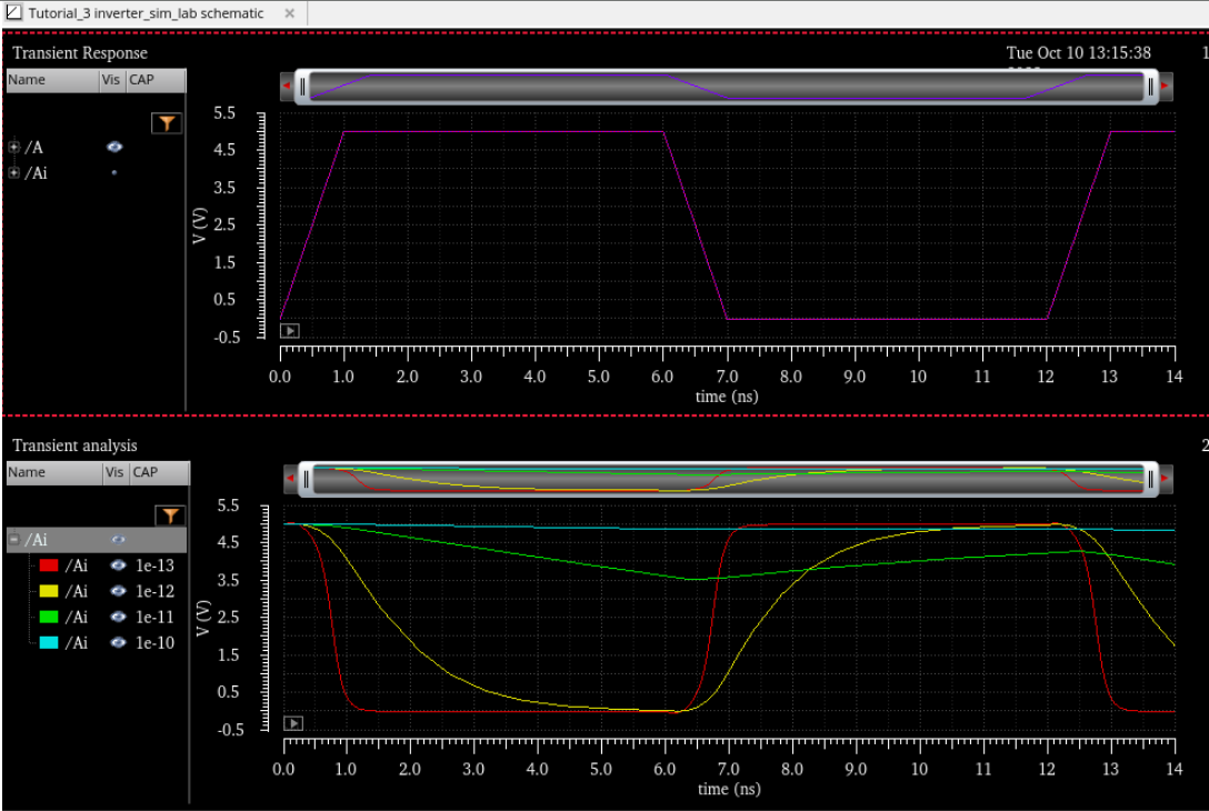
Simulation:
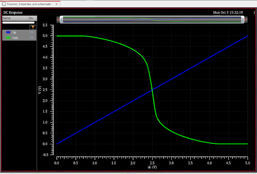
As you can see in this simulation, the inverter tries to get the exact
opposite output as the input. It isn't perfect because of parasitics
and general rules of MOSFETS and how they operate in saturation,
cutoff, etc.
Lab Work:
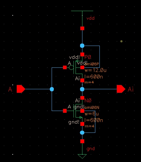
I was requiredto draft schematics layouts and symbols for inverters that were made with MOSFETS of different sizes
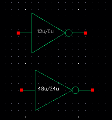
I created a 12u/6u version, as well as a 48u/24u, this device used a multiplier of M = 4.
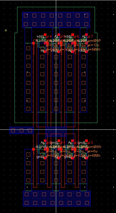
Schematics and symbols (notice the multiplier is four on the second image, which is the 48u/24u symbol):
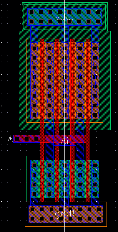
Layouts, Extractions:
12u/6u:
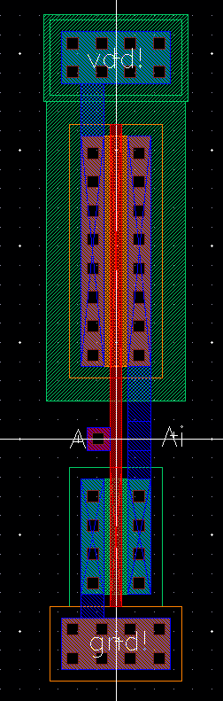
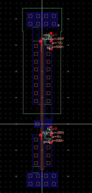
48u/24u:
DRC and LVS of the two inverters:
12u/6u:
48u/24u:
 \
\
Next in the lab, we had to
simulate the inverters we created with different capacitive loads. This
was done in two ways, using the typical spectre analysis (we have done
this before), and using ultrasim:
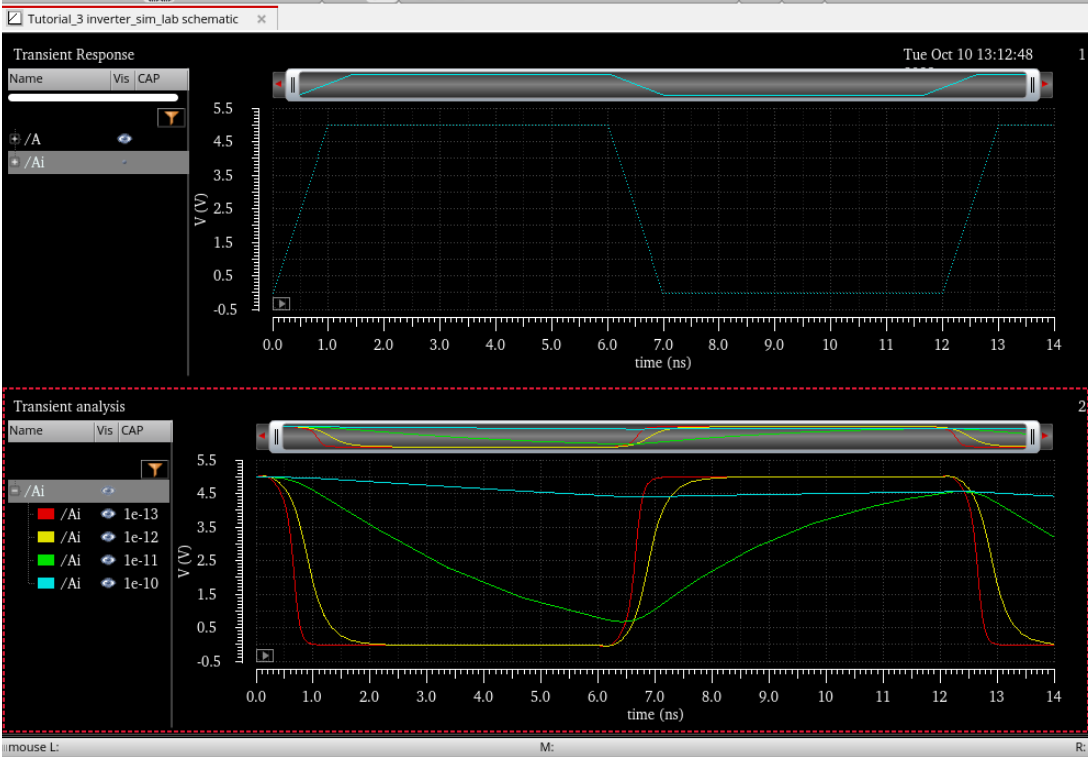
12/6u simulations and schem:
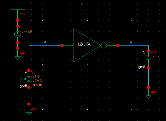
Spectre:
Ultrasim:
48/24u simulations and schem:
Spectre:
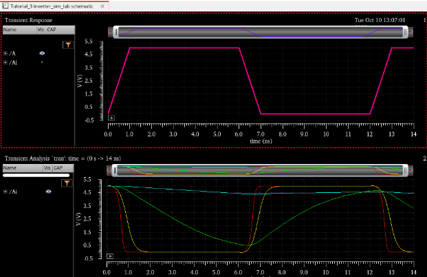
Ultrasim:
Additinoally, I backed up and zipped all my files. They can be found here:
lab5_bzv.zip
Return to all of Batya's Labs