Lab 4 - ECE 421L
Authored
by Batya Vishnepolsky, vishnepo@unlv.nevada.edu
9/26/23
Lab
description
in
this lab we learn about the layours of an NMOS and PMOS transistor in the C5process.
Prelab Description
I backed up all my work from the labs as seen in previous lab reports.
I read through the lab before starting it,
And then I had to go through
tutorial #2 on Dr. Baker's website, which walks you through NMOS and
PMOS schematic, symbol, and layout generation. Below are a few snippits
of what I did in tutorial 2:
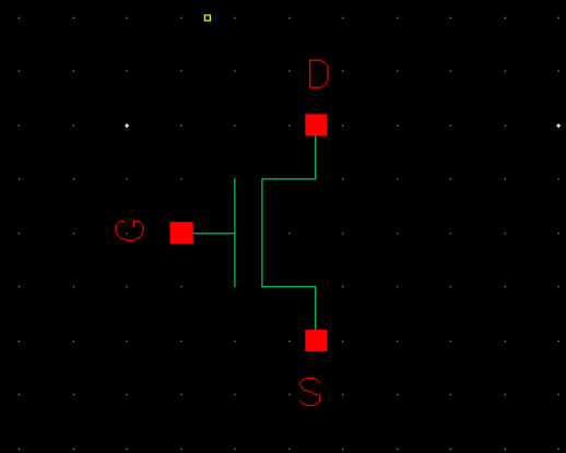
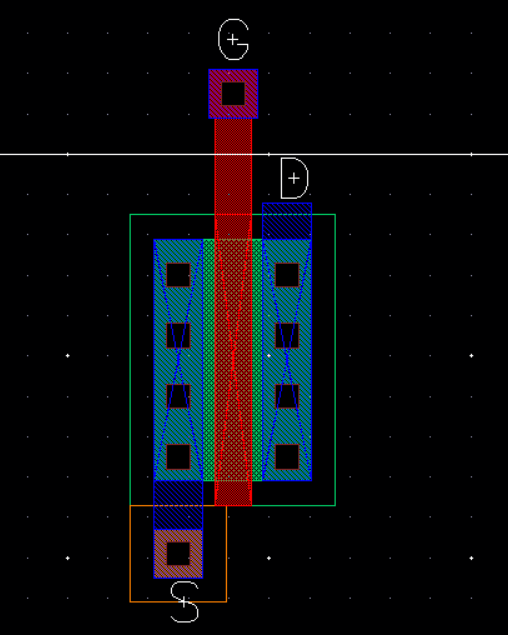
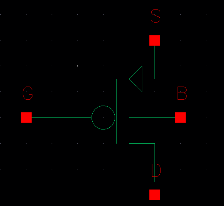
NMOS Symbol and Layout:
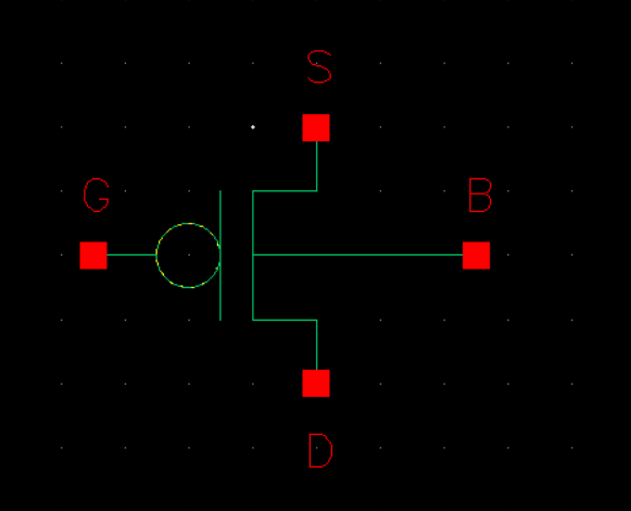
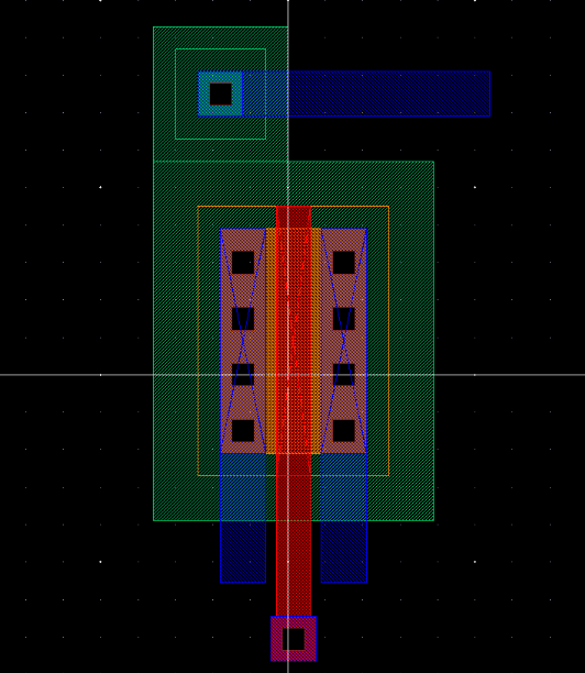
PMOS Symbol and Layout:
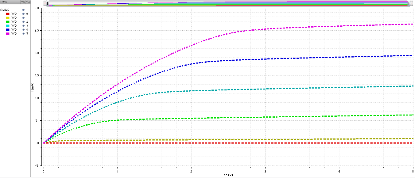
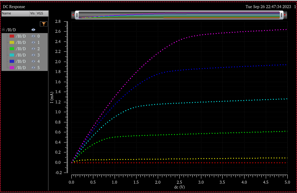
IV Curves NMOS responce:
Lab Work:
The first thing I had to do for this lab was make a probe pad, which was done using cells found in the lab4.zip

I then made the PMOS and NMOS schematics and symbols for the schematics as well:
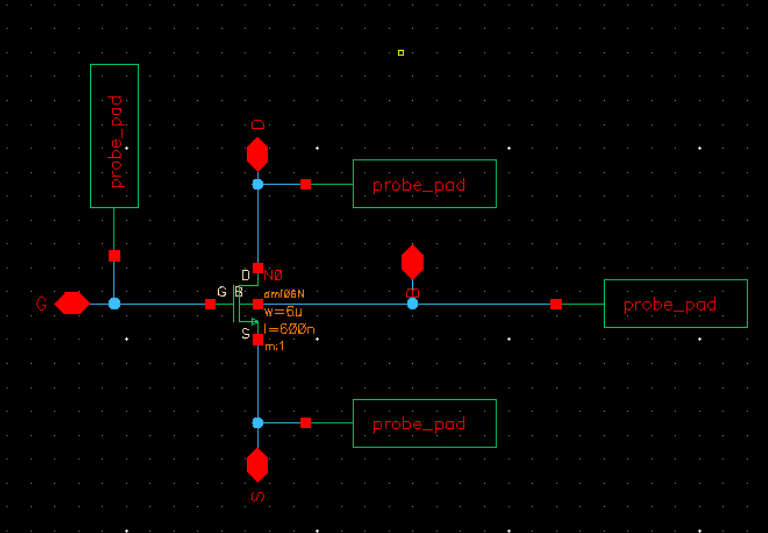
NMOS:
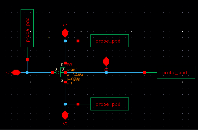
PMOS:
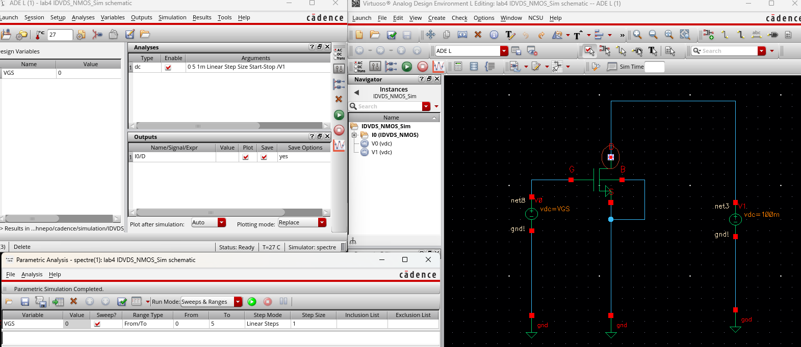
Next, I needed to create four different simulations accrding to the lab requirements:
I took the NMOS symbol I
generated and put it into simulation schematic, so that I could attach
voltages to them. In both simulations, VGS varies from 0-5 in steps of
1 Volt, and VDS varies from 0 - 5 in 1mV steps in this initial
simulation:
NMOS Schem and results:
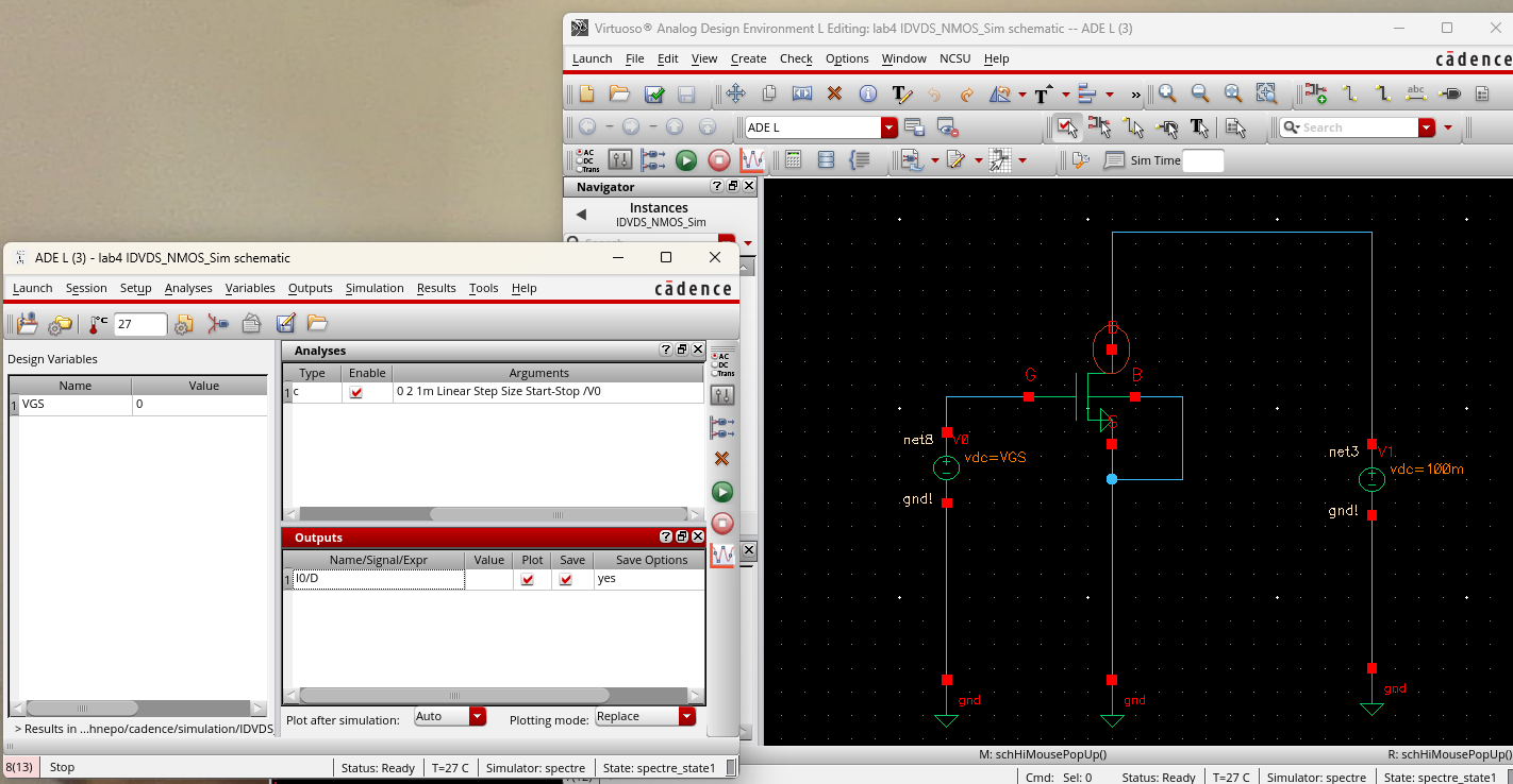
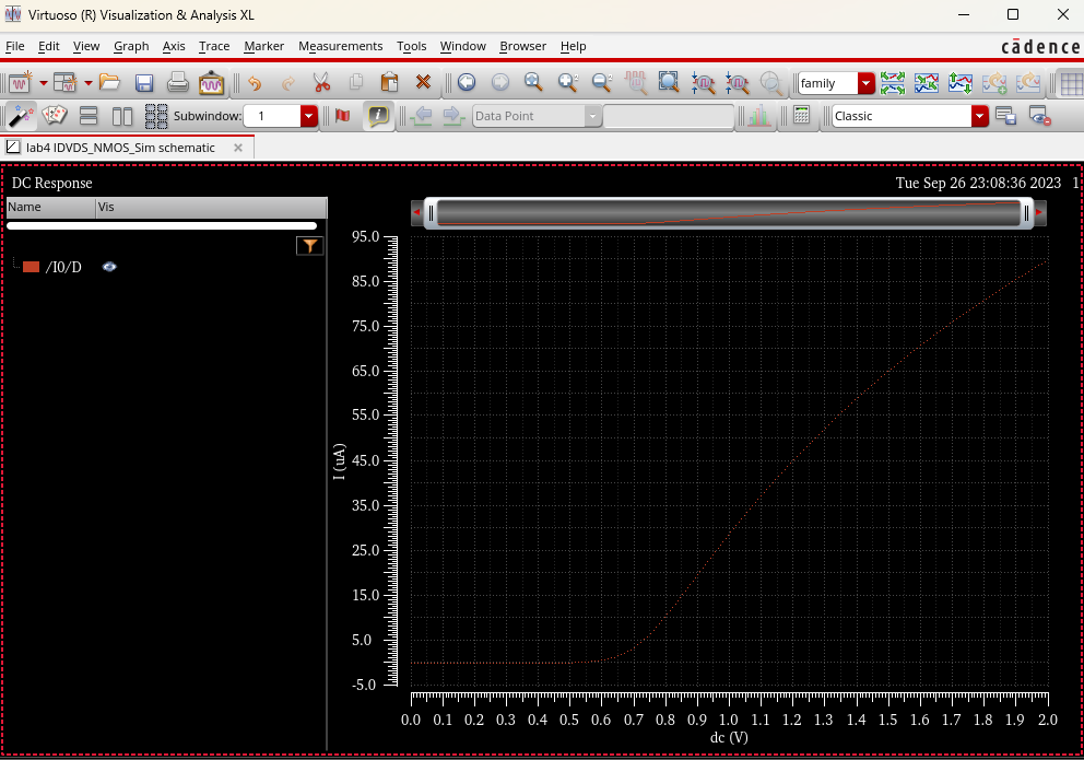
In this next simulation, I use an NMOS for VDS = 100mV, and VGS os varying from 0-2V in 1mV steps:
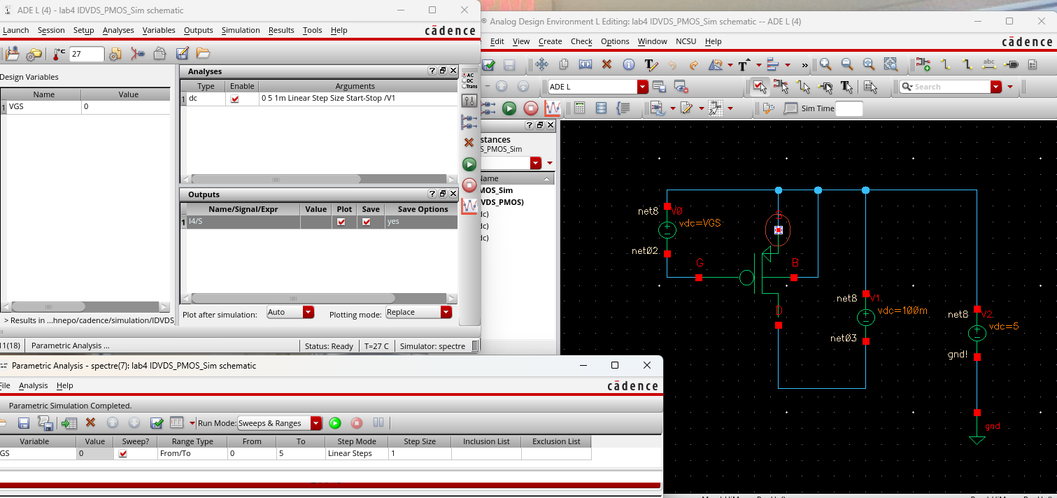
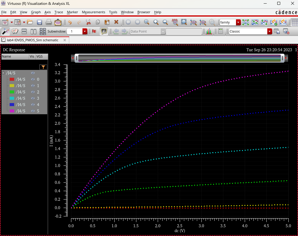
In this simulation, I use a
PMOS and vary the voltage from 0-5 in VSG from 0-5 in 1 volt steps, and
vary VSD from 0 - 5 in 1mV steps:
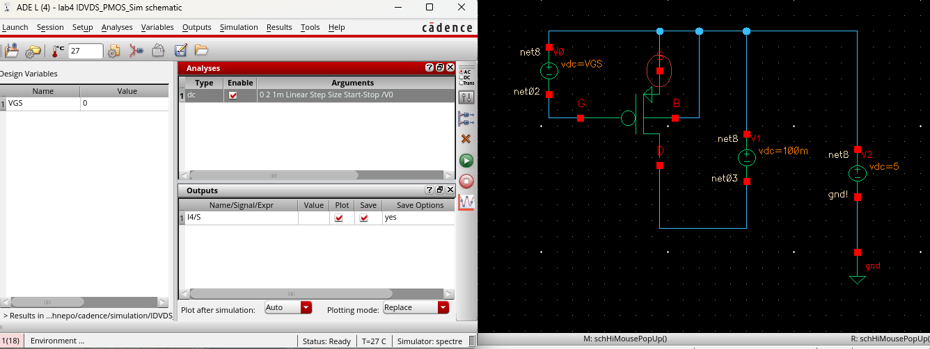
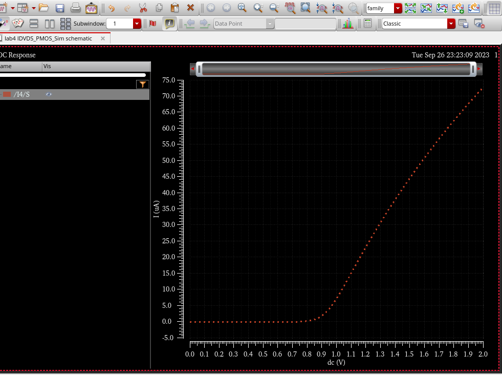
And in this last one, I still use a PMOS and vary toe VSG from 0 - 2V in 1mV steps
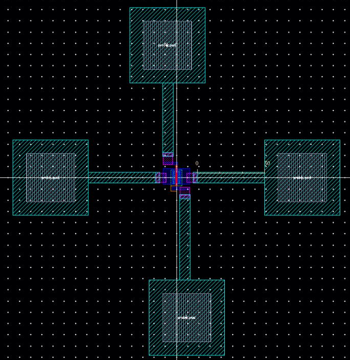
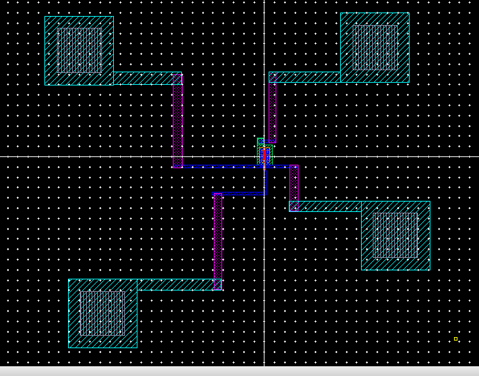
Next part of the lab consisted of doing layouts of the NMOS and PMOS device with probe pads that are included in the lab4.zip
First, I will do the NMOS device.
As seen earlier in the lab, I premade the schematics attached with the
probe pins. I will show this again. The symbol that we use will be the
same as well:
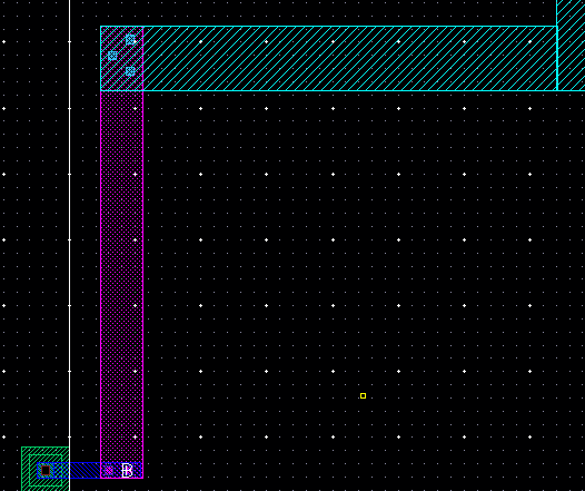
Layout:
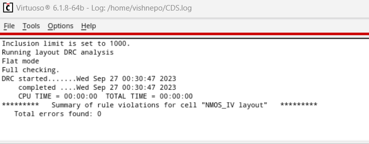
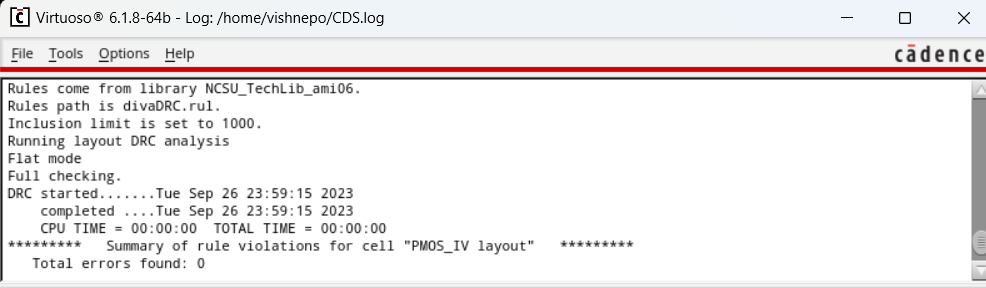
DRC:
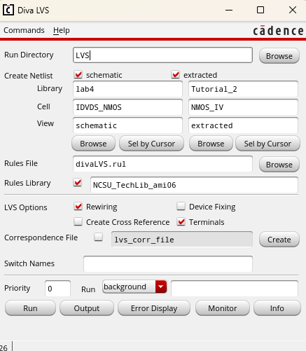
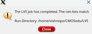
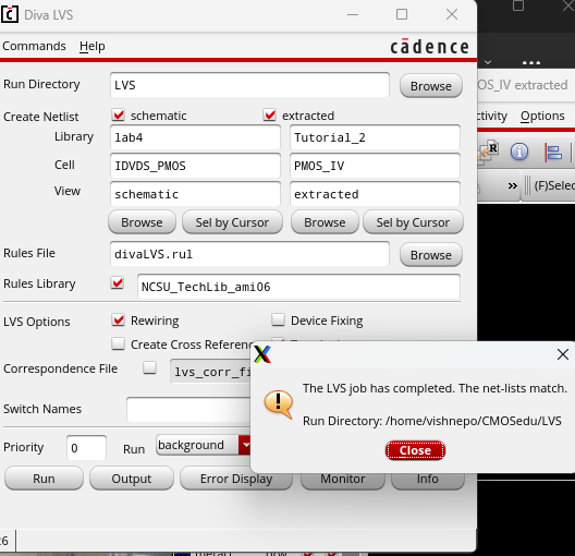
And then I extract and LVS:
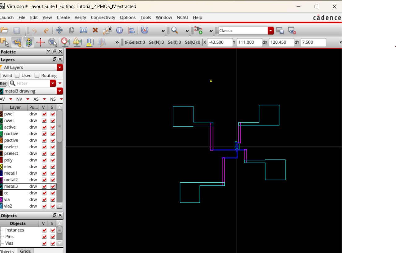
Now for the PMOS. The schematic and symbol are already made as well as seen below.
Now we will make the layout:
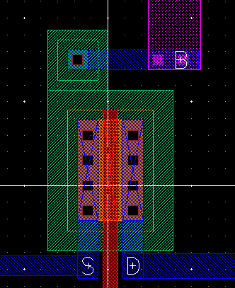
Zoomed in views of the PMOS and the pad connectivities (similar method to NMOS)
DRC:
Extract:
LVS:
And thats the end of my lab. As usual, I always zip and back up my work :)
Return to all of Batya's Labs