Lab 3 - ECE 421L
Authored
by Batya Vishnepolsky, vishnepo@unlv.nevada.edu
9/19/23
Prelab Content
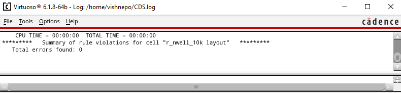
In the prelab I had to complete tutorial 1, here is a picture of the layout and DRC (design rule check) pass.
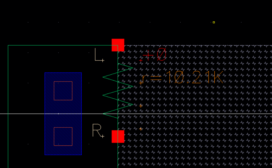
Here is the extracted layout of an n-well resistor, it shows a resistance close to 10k
Next, I created a layout and also DRC'd my design, as instructed by my TA.
Clean DRC check:
Additionally,
I backed up all my work from previous labs. The work was backed up and
emailed to myself, you can find this information in previous labs. Each
one of those labs includes a screenshot at the end of the backups.
Actual Lab Content:
Picking a Length and Width for my n-well resistor:
In
order to figure out the length and width of a resistor, one must know
the resistance that they need to create. Since we are creating a 10k
resistor in this lab, we have to design around those specifications.
When using the C5 process, there is a MOSIS parameter file that
contains information relevent to the design constraints as well. The
file lists the sheet resistance, which changes affects the resistance.
The sheet is resistance is 855 ohms per square. Additionally, the
minimum width is 12 lambda, which is about 3um. We then establish that
the minimum width is 3.6microns. Using these values, we can establish
that
Resistance = Sheet_resistance * l/w. Therefore, l = Resistance*w / Sheet_resistance = 10k * 3.6um/ 855 = about 42um.
The
ideal length will be 42 microns, but because I was following Dr.
Baker's Tutorial 1, I chose to stick with his dimensions of 56.1um
length and width of 4.5 (This will still get us the desired resistance,
because the ratio of l/w is roughly the same result.
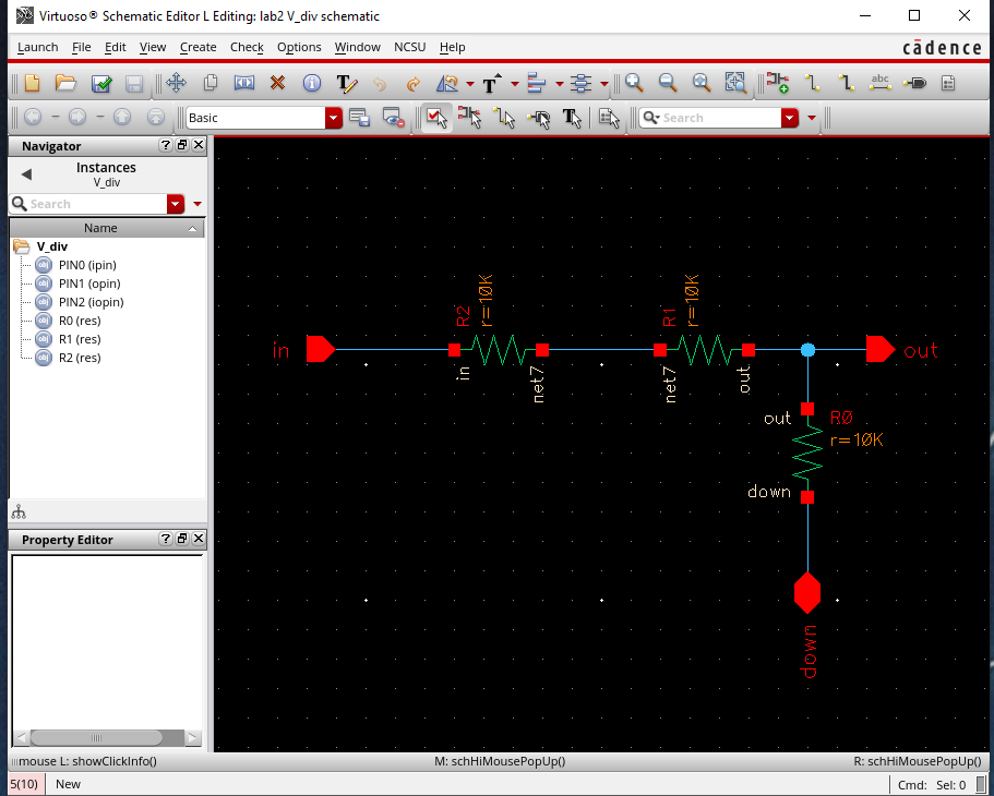
Measuring the resistor:
You
can go ahead and measure the resistor as well using bindkey K in layout
window, as you can see below, the resistor is roughly 56.1 microns by
4.5 microns
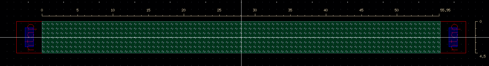
Additionally, this resistor passes a DRC check, as seen below:
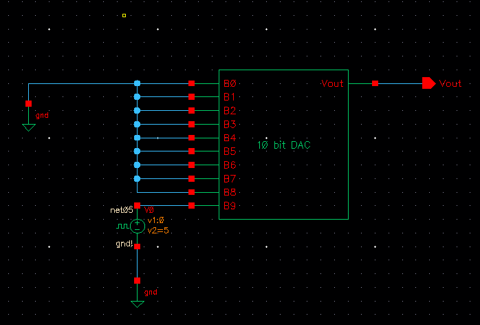
In
order to make a DAC using n-well resistors, I looked back at my
functioning DAC from lab 2 and saw that I needed a total of 31
resistors to make a 10 bit DAC. My DAC was 10 voltage dividers
combined, and in each divider there were three reistors (total of 30).
the extra resistor is found at the bottom of the voltage dividers. (The
picture below are directly taken from lab2)
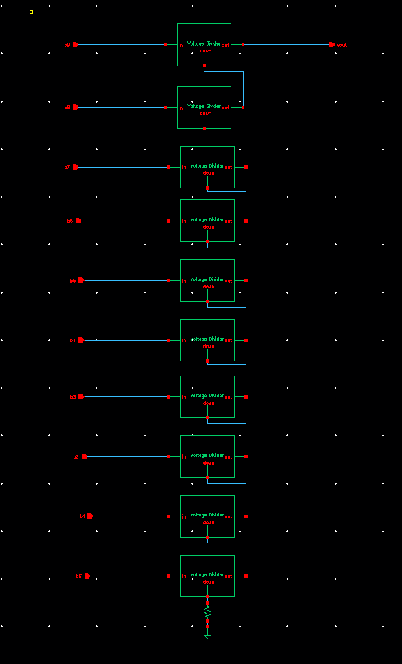
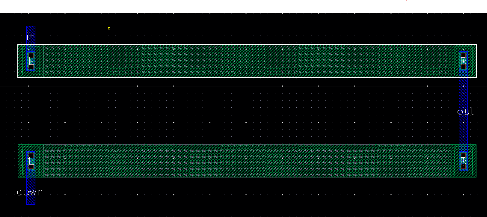
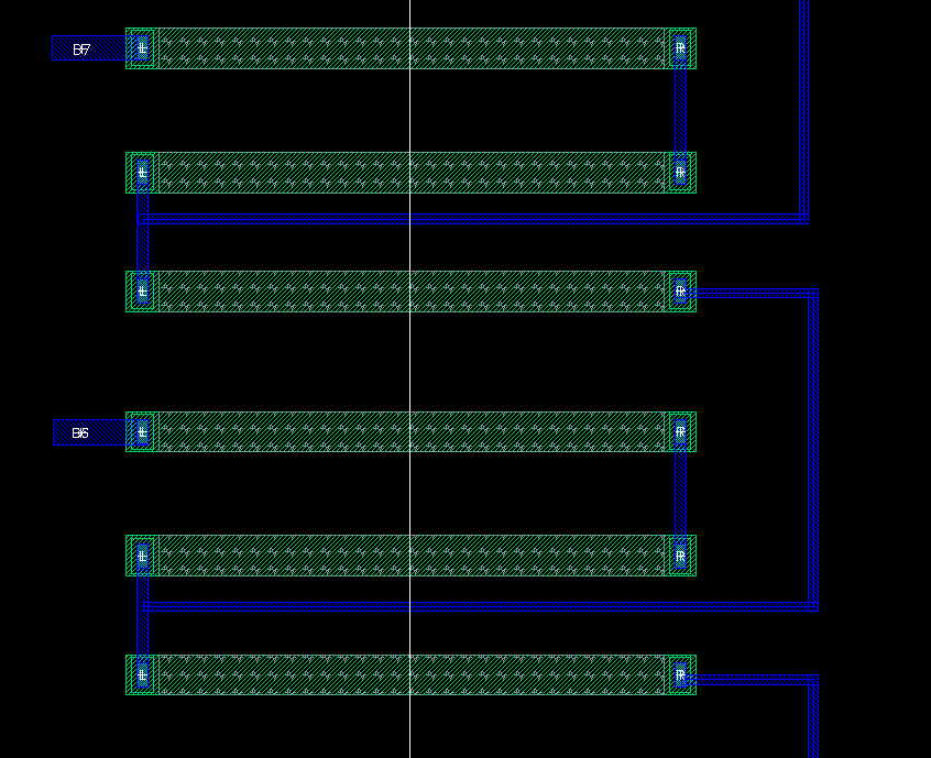
Next,
I layed out all 31 resistors at the same x coordinate, but varying y
positions. I had to ensure that there was enough space betwen the
resistors in order to not trigger any of the DRC design rules. I
included the overall screenshot, as well as a closer look at how the
voltage dividers were wired. Basically, three resistors create
one voltage divider--so there is a binary input seen at every three
resistors, one for every voltage divider. The Vdividers are wired to
each other. On the bottom there is a final resistor as well.
Furthermore, Vout was put in the right spot -- after the second
resistor in the entire layout. 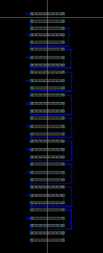
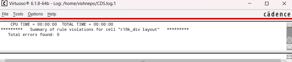
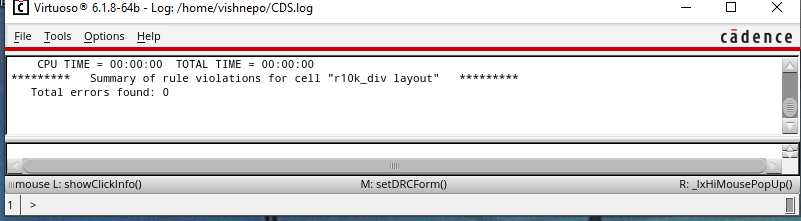
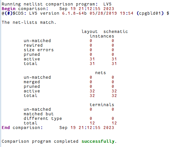
Next I had to do a DRC and LVS to ensure that this matched my DAC that I designed in previous labs.
DRC:
LVS:
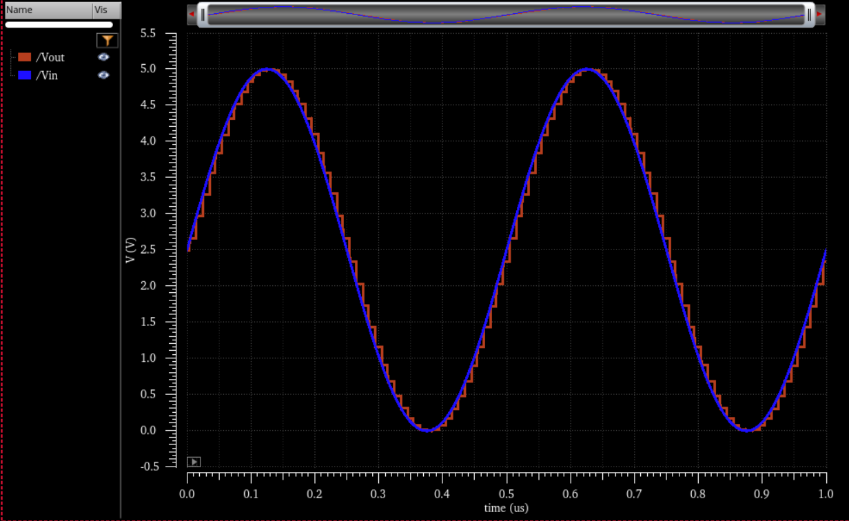
The DAC looks like, and will give a simulation that looks like this:
I also compressed all my work into a zip file, which is linked here
Return to all of Batya's Labs